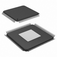
SCAN25100TYA/NOPB National Semiconductor, SCAN25100TYA/NOPB Datasheet - Page 8

SCAN25100TYA/NOPB
Manufacturer Part Number
SCAN25100TYA/NOPB
Description
IC SERIAL/DESERIAL CPRI 100-TQFP
Manufacturer
National Semiconductor
Series
SCANr
Datasheet
1.SCAN25100TYANOPB.pdf
(34 pages)
Specifications of SCAN25100TYA/NOPB
Function
Serializer/Deserializer
Data Rate
2.5Gbps
Input Type
LVTTL/LVCMOS
Output Type
LVTTL, LVCMOS
Number Of Inputs
10
Number Of Outputs
10
Voltage - Supply
1.7 V ~ 1.9 V
Operating Temperature
-40°C ~ 85°C
Mounting Type
Surface Mount
Package / Case
100-TQFP Exposed Pad, 100-eTQFP, 100-HTQFP, 100-VQFP
Operating Temperature (min)
-40C
Operating Temperature Classification
Industrial
Operating Temperature (max)
85C
Package Type
TQFP EP
Rad Hardened
No
Lead Free Status / RoHS Status
Lead free / RoHS Compliant
Other names
SCAN25100TYA
Available stocks
Company
Part Number
Manufacturer
Quantity
Price
Company:
Part Number:
SCAN25100TYA/NOPB
Manufacturer:
NS
Quantity:
158
Company:
Part Number:
SCAN25100TYA/NOPB
Manufacturer:
Texas Instruments
Quantity:
10 000
www.national.com
JTAG DC SPECIFICATIONS (3.3V I/O)
V
V
I
V
V
C
MDIO/MDC/ADD0-4 DC SPECIFICATIONS
V
V
I
V
V
I
C
POWER CONSUMPTION
P
POWER CONSUMPTION (Powerdown)
P
TYPICAL POWER CONSUMPTION (By Supply)
P
RECOMMENDED REFCLK INPUT SPECIFICATIONS
V
V
f
df
t
t
SYSCLK DC OUTPUT SPECIFICATIONS
V
V
I
I
IN
IN
OZ
REF
REF-DC
REF-X
OS
OZ
IH
IL
OH
OL
IH
IL
OH
OL
D
PDN
DS
IDSREFCLK
ICM
OD
OS
IO
IO
Symbol
REF
High level input voltage
Low level input voltage
Input Current
High level output voltage
Low level output voltage
Input/Output Capacitance
High level input voltage
Low level input voltage
Input Current
High level output voltage
Low level output voltage
Power Down Output Current
Input/Output Capacitance
Max total power consumption
PRWS pattern embedded in
hyperframe
Output loading:
CML: AC-coupled
CMOS: 50Ω
Powerdown Mode
PVDD33
AVDD33
IOVDD
AVDD18
Differential input voltage
Common mode voltage
REFCLK frequency
REFCLK frequency variation
REFCLK duty cycle
REFCLK transition time
Differential Output Voltage
Offset Voltage
Output Short Circuit Current
Power Down Output Current
Parameter
transmission line
V
I
I
Typical
V
I
I
Power down
Typical
614.4 Mbps
Parallel I/O at 1.9V
Parallel I/O at 3.465V
1228.8 Mbps
Parallel I/O at 1.9V
Parallel I/O at 3.465V
2457.6 Mbps
Parallel I/O at 1.9V
Parallel I/O at 3.465V
Rx and Tx Powerdown
2457.6 Mbps operation
Parallel I/O at 3.3V
PRWS pattern embedded in
hyperframe
OPMODE = 0 (BTS SerDes Mode)
Variation from nominal frequency
Between 50% of the differential
voltage across REFCLKP and
REFCLKN
Transition time between 20% and
80% of the differential voltage
across REFCLKP and REFCLKN
R
Output pair shorted together and
tied to GND
Power down
OH
OL
OH
OL
IN
IN
L
= 100Ω
= 2 mA
= 2 mA
= −2 mA
= −2 mA
= 0V or 3.465V
= 0V or 3.465V
Condition
8
0.05V
± 100
± 250
1.125
GND
−100
−100
-150
Min
−35
−30
2.4
2.0
2.4
30
45
2
(Note 2)
± 330
30.72
1040
1110
1020
1230
1.20
Typ
920
950
315
175
255
485
300
2.8
2.8
25
3.465
± 450
1.375
+150
+100
1040
1150
1100
1250
1200
1350
2.4V
Max
31.5
+35
100
+30
0.8
0.4
0.8
0.4
40
55
35
mV
Units
MHz
ppm
mW
mW
mW
mW
mW
mW
mW
mW
mW
mW
mW
mV
mA
µA
pF
µA
µA
pF
pS
µA
%
V
V
V
V
V
V
V
V
V
V
P-P


