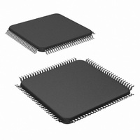
DS90CR482VS/NOPB National Semiconductor, DS90CR482VS/NOPB Datasheet

DS90CR482VS/NOPB
Specifications of DS90CR482VS/NOPB
DS90CR482VS
Available stocks
Related parts for DS90CR482VS/NOPB
DS90CR482VS/NOPB Summary of contents
Page 1
... Channel Link devices and offers higher band- width support and longer cable drive with three areas of Generalized Block Diagrams (DS90CR481 and DS90CR482) © 2006 National Semiconductor Corporation enhancement. To increase bandwidth, the maximum clock rate is increased to 112 MHz and 8 serialized LVDS outputs are provided ...
Page 2
Generalized Transmitter Block Diagram – DS90CR481 Generalized Receiver Block Diagram – DS90CR482 Ordering Information Order Number DS90CR481VJD DS90CR482VS www.national.com Function Transmitter (Serializer) Receiver (Deserializer) 2 20009102 20009103 Package VJD100A VJD100A ...
Page 3
... Absolute Maximum Ratings If Military/Aerospace specified devices are required, please contact the National Semiconductor Sales Office/ Distributors for availability and specifications. Supply Voltage ( CMOS/TTL Input Voltage LVCMOS/TTL Output Voltage −0. LVDS Receiver Input Voltage LVDS Driver Output Voltage LVDS Output Short Circuit Duration ...
Page 4
Electrical Characteristics Over recommended operating supply and temperature ranges unless otherwise specified. Symbol Parameter I Output Short Circuit OS Current I Output TRI-STATE OZ Current LVDS RECEIVER DC SPECIFICATIONS V Differential Input High TH Threshold V Differential Input Low TL ...
Page 5
Transmitter Switching Characteristics Over recommended operating supply and temperature ranges unless otherwise specified. Symbol Parameter LLHT LVDS Low-to-High Transition Time, (Figure 2), PRE = 0.75V (disabled) LVDS Low-to-High Transition Time, (Figure 2), PRE = Vcc (max) LHLT LVDS High-to-Low Transition ...
Page 6
Chipset RSKM Characteristics Over recommended operating supply and temperature ranges unless otherwise specified.(Notes 4, 7). See Applications Infor- mation section for more details on this parameter and how to apply it. Symbol Parameter RSKM Receiver Skew Margin without Deskew in ...
Page 7
AC Timing Diagrams Note 8: The worst case test pattern produces a maximum toggling of digital circuits, LVDS I/O and CMOS/TTL I/O. FIGURE 2. DS90CR481 (Transmitter) LVDS Output Load and Transition Times FIGURE 3. DS90CR482 (Receiver) CMOS/TTL Output Load and ...
Page 8
AC Timing Diagrams FIGURE 5. DS90CR481 (Transmitter) Setup/Hold and High/Low Times FIGURE 6. DS90CR482 (Receiver) Setup/Hold and High/Low Times FIGURE 7. DS90CR481 (Transmitter) Propagation Delay - Latency www.national.com (Continued) 8 20009115 20009131 20009127 ...
Page 9
AC Timing Diagrams (Continued) FIGURE 8. DS90CR482 (Receiver) Propagation Delay - Latency FIGURE 9. DS90CR481 (Transmitter) Phase Lock Loop Set Time FIGURE 10. DS90CR482 (Receiver) Phase Lock Loop Set Time 20009132 20009119 9 20009133 www.national.com ...
Page 10
AC Timing Diagrams FIGURE 11. DS90CR481 (Transmitter) Power Down Delay FIGURE 12. DS90CR482 (Receiver) Power Down Delay www.national.com (Continued) 10 20009121 20009134 ...
Page 11
AC Timing Diagrams (Continued) C — Setup and Hold Time (Internal data sampling window) defined by Rspos (receiver input strobe position) min and max Tppos — Transmitter output pulse position (min and max) RSKM ≥ Cable Skew (type, length) + ...
Page 12
LVDS Interface Optional features supported: Pre-emphasis and DESKEW FIGURE 15. 48 Parallel TTL Data Bits Mapped to LVDS Bits with DC Balance Enabled www.national.com 12 20009104 ...
Page 13
LVDS Interface (Continued) Optional feature supported: Pre-emphasis FIGURE 16. 48 Parallel TTL Data Bits Mapped to LVDS Bits with DC Balance Disabled 13 20009135 www.national.com ...
Page 14
Applications Information The DS90CR481/DS90CR482 chipset is improved over prior generations of Channel Link devices and offers higher band- width support and longer cable drive with three areas of enhancement. To increase bandwidth, the maximum clock rate is increased to 112 ...
Page 15
Applications Information current data disparity is zero or negative, the data shall be sent inverted. If the running word disparity is zero, the data shall be sent inverted. DC Balance mode is set when the BAL pin on the transmitter ...
Page 16
Applications Information HOW TO CONFIGURE FOR BACKPLANE APPLICATIONS In a backplane application with differential line impedance of 100Ω the differential line pair-to-pair skew can controlled by trace layout. The transmitter-DS90CR481 “DS_OPT” pin may be set high backplane application ...
Page 17
DS90CR481 Pin Descriptions—Channel Link Transmitter Pin Name I/O TxIN I TxOUTP O TxOUTM O TxCLKIN I TxCLKP O TxCLKM PLLSEL I PRE I DS_OPT I BAL GND I PLLV I CC PLLGND I ...
Page 18
DS90CR482 Pin Descriptions—Channel Link Receiver Pin Name I/O RxINP I RxINM I RxOUT O RxCLKP I RxCLKM I RxCLKOUT O PLLSEL I DESKEW GND I PLLV I CC PLLGND I LVDSV I CC LVDSGND ...
Page 19
DS90DR481 — Connection Diagram Transmitter - DS90CR481 - TQFP - Top View 19 20009106 www.national.com ...
Page 20
DS90CR482 – Connection Diagram www.national.com Receiver - DS90CR482 - TQFP - Top View 20 20009107 ...
Page 21
... BANNED SUBSTANCE COMPLIANCE National Semiconductor manufactures products and uses packing materials that meet the provisions of the Customer Products Stewardship Specification (CSP-9-111C2) and the Banned Substances and Materials of Interest Specification (CSP-9-111S2) and contain no ‘‘Banned Substances’’ as defined in CSP-9-111S2. ...


