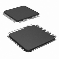
DS90CR482VS/NOPB National Semiconductor, DS90CR482VS/NOPB Datasheet - Page 6

DS90CR482VS/NOPB
Manufacturer Part Number
DS90CR482VS/NOPB
Description
IC SERIALIZER 48BIT 100-TQFP
Manufacturer
National Semiconductor
Datasheet
1.DS90CR481VJDNOPB.pdf
(21 pages)
Specifications of DS90CR482VS/NOPB
Function
Serializer/Deserializer
Data Rate
5.38Gbps
Input Type
LVDS
Output Type
CMOS, TTL
Number Of Inputs
8
Number Of Outputs
48
Voltage - Supply
3 V ~ 3.6 V
Operating Temperature
-10°C ~ 70°C
Mounting Type
Surface Mount
Package / Case
100-TQFP, 100-VQFP
Lead Free Status / RoHS Status
Lead free / RoHS Compliant
Other names
*DS90CR482VS
DS90CR482VS
DS90CR482VS
Available stocks
Company
Part Number
Manufacturer
Quantity
Price
Company:
Part Number:
DS90CR482VS/NOPB
Manufacturer:
Texas Instruments
Quantity:
10 000
www.national.com
RSKM
RSKM
RSKMD
RDR
RDSS
Symbol
Chipset RSKM Characteristics
Over recommended operating supply and temperature ranges unless otherwise specified.(Notes 4, 7). See Applications Infor-
mation section for more details on this parameter and how to apply it.
Note 1: “Absolute Maximum Ratings” are those values beyond which the safety of the device cannot be guaranteed. They are not meant to imply that the device
should be operated at these limits. The tables of “Electrical Characteristics” specify conditions for device operation.
Note 2: Typical values are given for V
Note 3: Current into device pins is defined as positive. Current out of device pins is defined as negative. Voltages are referenced to ground unless otherwise
specified (except V
Note 4: The Minimum and Maximum Limits are based on statistical analysis of the device performance over voltage and temperature ranges. This parameter is
functionally tested on Automatic Test Equipment (ATE). ATE is limited to 85MHz. A sample of characterization parts have been bench tested to verify functional
performance.
Note 5: Receiver Skew Margin (RSKM) is defined as the valid data sampling region at the receiver inputs. This margin takes into account transmitter output pulse
positions (min and max) and the receiver input setup and hold time (internal data sampling window, RSPOS). This margin allows for LVDS interconnect skew,
inter-symbol interference (both dependent on type/length of cable) and clock jitter (TJCC).
RSKM ≥ cable skew (type, length) + source clock jitter (cycle to cycle,TJCC) + ISI (if any). See Applications Information section for more details.
Note 6: Receiver Skew Margin with Deskew (RSKMD) is defined as the valid data sampling region at the receiver inputs. The DESKEW function will constrain the
receiver’s sampling strobes to the middle half of the LVDS bit and removes (adjusts for) fixed interconnect skew. This margin (RSKMD) allows for inter-symbol
interference (dependent on type/length of cable), Transmitter Pulse Position (TPPOS) variance, and LVDS clock jitter (TJCC).
RSKMD ≥ ISI + TPPOS(variance) + source clock jitter (cycle to cycle, TJCC). See Applications Information section for more details.
Note 7: Typical values for RSKM and RSKMD are applicable for fixed V
T
A
points).
Receiver Skew Margin without
Deskew in non-DC Balance Mode,
(Figure 13), (Note 5)
Receiver Skew Margin without
Deskew in DC Balance Mode,
(Figure 13), (Note 5)
Receiver Skew Margin with Deskew
in DC Balance, (Figure 14),
(Note 6)
Receiver Deskew Range
Receiver Deskew Step Size
TH
, V
TL
, V
OD
and ∆V
CC
OD
Parameter
= 3.3V and T
).
A
= +25˚C.
f = 112 MHz
f = 100 MHz
f = 85MHz
f = 66MHz
f = 112 MHz
f = 100 MHz
f = 85 MHz
f = 66 MHz
f = 33 to 80
MHz
f = 80 MHz
f = 80 MHz
CC
and T
6
A
of the Transmitter and Receiver (both are assumed to be at the same V
0.25TBIT
Min
170
170
300
300
170
170
250
250
±
1
0.3 TBIT
Typ
240
350
350
200
300
300
Max
CC
Units
TBIT
ps
ps
ps
ps
ps
ps
ps
ps
ps
ns
and


