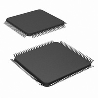
DS90CR482VS/NOPB National Semiconductor, DS90CR482VS/NOPB Datasheet - Page 17

DS90CR482VS/NOPB
Manufacturer Part Number
DS90CR482VS/NOPB
Description
IC SERIALIZER 48BIT 100-TQFP
Manufacturer
National Semiconductor
Datasheet
1.DS90CR481VJDNOPB.pdf
(21 pages)
Specifications of DS90CR482VS/NOPB
Function
Serializer/Deserializer
Data Rate
5.38Gbps
Input Type
LVDS
Output Type
CMOS, TTL
Number Of Inputs
8
Number Of Outputs
48
Voltage - Supply
3 V ~ 3.6 V
Operating Temperature
-10°C ~ 70°C
Mounting Type
Surface Mount
Package / Case
100-TQFP, 100-VQFP
Lead Free Status / RoHS Status
Lead free / RoHS Compliant
Other names
*DS90CR482VS
DS90CR482VS
DS90CR482VS
Available stocks
Company
Part Number
Manufacturer
Quantity
Price
Company:
Part Number:
DS90CR482VS/NOPB
Manufacturer:
Texas Instruments
Quantity:
10 000
DS90CR481 Pin Descriptions—Channel Link Transmitter
Note 10: Inputs default to “low” when left open due to internal pull-down resistor.
TxIN
TxOUTP
TxOUTM
TxCLKIN
TxCLKP
TxCLKM
PD
PLLSEL
PRE
DS_OPT
BAL
V
GND
PLLV
PLLGND
LVDSV
LVDSGND
NC
CC
Pin Name
CC
CC
I/O
O
O
O
O
I
I
I
I
I
I
I
I
I
I
I
I
I
TTL level input. (Note 10).
Positive LVDS differential data output.
Negative LVDS differential data output.
TTL level clock input. The rising edge acts as data strobe.
Positive LVDS differential clock output.
Negative LVDS differential clock output.
TTL level input. Assertion (low input) tri-states the outputs, ensuring low
current at power down. (Note 10).
PLL range select. This pin must be tied to V
reserved for future use. (Note 10)
Pre-emphasis “level” select. Pre-emphasis is active when input is tied to V
through external pull-up resistor. Resistor value determines Pre-emphasis
level (See Applications Information Section). For normal LVDS drive level
(No Pre-emphasis) leave this pin open (do not tie to ground).
Cable Deskew performed when TTL level input is low. No TxIN data is
sampled during Deskew. To perform Deskew function, input must be held
low for a minimum of 4 clock cycles. The Deskew operation is normally
conducted after the TX and RX PLLs have locked. It should also be
conducted after a system reset, or a reconfiguration event. It must be
peformed at least once when "DESKEW" is enabled. (Note 10)
TTL level input. This pin was previously labeled as V
DC Balance function. But when tied low or left open, the DC Balance
function is disabled. Please refer to (Figures 15, 16) for LVDS data bit
mapping respectively. (Note 10), (Note 12)
Power supply pins for TTL inputs and digital circuitry. Bypass not required
on Pins 20 and 21.
Ground pins for TTL inputs and digital circuitry.
Power supply pin for PLL circuitry.
Ground pins for PLL circuitry.
Power supply pin for LVDS outputs.
Ground pins for LVDS outputs.
No Connect. Make NO Connection to these pins - leave open.
17
Description
CC
. NC or tied to Ground is
CC
, which enabled the
www.national.com
CC


