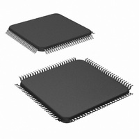
DS90CR482VS/NOPB National Semiconductor, DS90CR482VS/NOPB Datasheet - Page 16

DS90CR482VS/NOPB
Manufacturer Part Number
DS90CR482VS/NOPB
Description
IC SERIALIZER 48BIT 100-TQFP
Manufacturer
National Semiconductor
Datasheet
1.DS90CR481VJDNOPB.pdf
(21 pages)
Specifications of DS90CR482VS/NOPB
Function
Serializer/Deserializer
Data Rate
5.38Gbps
Input Type
LVDS
Output Type
CMOS, TTL
Number Of Inputs
8
Number Of Outputs
48
Voltage - Supply
3 V ~ 3.6 V
Operating Temperature
-10°C ~ 70°C
Mounting Type
Surface Mount
Package / Case
100-TQFP, 100-VQFP
Lead Free Status / RoHS Status
Lead free / RoHS Compliant
Other names
*DS90CR482VS
DS90CR482VS
DS90CR482VS
Available stocks
Company
Part Number
Manufacturer
Quantity
Price
Company:
Part Number:
DS90CR482VS/NOPB
Manufacturer:
Texas Instruments
Quantity:
10 000
www.national.com
Applications Information
HOW TO CONFIGURE FOR BACKPLANE
APPLICATIONS
In a backplane application with differential line impedance of
100Ω the differential line pair-to-pair skew can controlled by
trace layout. The transmitter-DS90CR481 “DS_OPT” pin
may be set high. In a backplane application with short PCB
distance traces, pre-emphasis from the transmitter is typi-
cally not required. The “PRE” pin should be left open (do not
tie to ground). A resistor pad provision for a pull up resistor to
Vcc can be implemented in case pre-emphasis is needed to
counteract heavy capacitive loading effects.
HOW TO CONFIGURE FOR CABLE INTERCONNECT
APPLICATIONS
In applications that require the long cable drive capability.
The DS90CR481/DS90CR482 chipset is improved over prior
generations of Channel Link devices and offers higher band-
width support and longer cable drive with the use of DC
balanced data transmission, pre-emphasis. Cable drive is
enhanced with a user selectable pre-emphasis feature that
provides additional output current during transitions to coun-
teract cable loading effects. This requires the use of one pull
up resistor to Vcc; please refer to Table 1 to set the level
needed. Optional DC balancing on a cycle-to-cycle basis, is
also provided to reduce ISI (Inter-Symbol Interference) for
long cable applications. With pre-emphasis and DC balanc-
ing, a low distortion eye-pattern is provided at the receiver
end of the cable. These enhancements allow cables 5+
meters in length to be driven. Depending upon clock rate and
the media being driven, the cable Deskew feature may also
be employed - see discussion on DESKEW, RSKM and
RSKMD above.
SUPPLY BYPASS RECOMMENDATIONS
Bypass capacitors must be used on the power supply pins.
Different pins supply different portions of the circuit, there-
fore capacitors should be nearby all power supply pins ex-
cept as noted in the pin description table. Use high fre-
quency ceramic (surface mount recommended) 0.1µF
capacitors close to each supply pin. If space allows, a
0.01µF capacitor should be used in parallel, with the small-
est value closest to the device pin. Additional scattered
capacitors over the printed circuit board will improve decou-
pling. Multiple (large) via should be used to connect the
decoupling capacitors to the power plane. A 4.7 to 10 µF bulk
cap is recommended near the PLLVCC pins and also the
LVDSVCC (pin #40) on the Transmitter. Connections be-
tween the caps and the pin should use wide traces.
INPUT SIGNAL QUALITY REQUIREMENTS -
TRANSMITTER
The input signal quality must comply to the datasheet re-
quirements, please refer to the "Recommended Transmitter
(Continued)
16
Input Characteristics" table for specifications. In addition
undershoots in excess of the ABS MAX specifications are
not recommended. If the line between the host device and
the transmitter is long and acts as a transmission line, then
termination should be employed. If the transmitter is being
driven from a device with programmable drive strengths,
data inputs are recommended to be set to a weak setting to
prevent transmission line effects. The clock signal is typically
set higher to provide a clean edge that is also low jitter.
UNUSED LVDS OUTPUTS
Unused LVDS output channels should be terminated with
100 Ohm at the transmitter’s output pin.
LVDS INTERCONNECT GUIDELINES
See AN-1108 and AN-905 for full details.
• Use 100Ω coupled differential pairs
• Use the S/2S/3S rule in spacings
• Minimize the number of VIA
• Use differential connectors when operating above
• Maintain balance of the traces
• Minimize skew within the pair
• Minimize skew between pairs
• Terminate as close to the RXinputs as possible
RECEIVER OUTPUT DRIVE STRENGTH
The DS90CR482 output specify a 8pF load, V
are tested at
2 loads. If high fan-out is required or long transmission line
driving capability, buffering the receiver output is recom-
mended. Receiver outputs do not support / provide a TRI-
STATE function.
DS90CR483/484
The DS90CR481/2 chipset is electrically similar to the
DS90CR483/4. The DS90CR481/2 differ only in the control
circuit of the internal PLL and are specified for 65 to 112 MHz
operation. The devices will directly inter-operate within the
scope of the respective datasheets.
FOR MORE INFORMATION
Channel Link Applications Notes currently available:
• AN-1041 Introduction to Channel Link
• AN-1059 RSKM Calculations
• AN-1108 PCB and Interconnect Guidelines
• AN-905 Differential Impedance
• National’s LVDS Owner’s Manual
— S = space between the pair
— 2S = space between pairs
— 3S = space to TTL signal
500Mbps line speed
±
2mA, which is intended for only 1 or maybe
OH
and V
OL


