PI7C9X7958ANBE Pericom Semiconductor, PI7C9X7958ANBE Datasheet
PI7C9X7958ANBE
Specifications of PI7C9X7958ANBE
Available stocks


Related parts for PI7C9X7958ANBE

PI7C9X7958ANBE Summary of contents
Page 1
PCI Express® Octal UART 11-0039 PI7C9X7958 Datasheet Revision 1.4 March 2011 3545 North 1ST Street, San Jose, CA 95134 Telephone: 1-877-PERICOM, (1-877-737-4266) FAX: 408-435-1100 Internet: http://www.pericom.com ...
Page 2
... Pericom Semiconductor does not assume any responsibility for use of any circuitry described other than the circuitry embodied in a Pericom Semiconductor product. The Company makes no representations that circuitry described herein is free from patent infringement or other rights of third parties which may result from its use ...
Page 3
... March 2011 – Revision 1.4 Pericom Semiconductor 11-0039 Description Preliminary Datasheet Fixed the diagrams Corrected Chapter 4.2 Pin Description (RREF, GPIO[7] EEPROM Organization Pin, RTS[0] EEPROM Bypass Pin) Updated Chapter 6 PCI Express Registers(6.2.42 [3], 6.2.36 UART Driver Setting, 6 ...
Page 4
... BASE ADDRESS REGISTER 0 – OFFSET 10h.....................................................................27 6.2.11. BASE ADDRESS REGISTER 1 – OFFSET 14h.....................................................................27 6.2.12. SUBSYSTEM VENDOR REGISTER – OFFSET 2Ch ............................................................27 6.2.13. SUBSYSTEM ID REGISTER – OFFSET 2Ch........................................................................27 March 2011 – Revision 1.4 Pericom Semiconductor 11-0039 PCI Express® Octal UART Page PI7C9X7958 Datasheet ...
Page 5
... CORRECTABLE ERROR MASK REGISTER – OFFSET 114h .............................................41 6.2.64. ADVANCE ERROR CAPABILITIES AND CONTROL REGISTER – OFFSET 118h.............42 6.2.65. HEADER LOG REGISTER – OFFSET From 11Ch to 128h .................................................42 March 2011 – Revision 1.4 Pericom Semiconductor 11-0039 PCI Express® Octal UART Page PI7C9X7958 Datasheet ...
Page 6
... LINE STATUS FIFO REGISTERS –OFFSET 180h ~ 1FFh ..................................................63 8. EEPROM INTERFACE .....................................................................................................................64 8.1. AUTO MODE EERPOM ACCESS ...............................................................................................64 8.2. EEPROM MODE AT RESET ........................................................................................................64 8.3. EEPROM SPACE ADDRESS MAP AND DESCRIPTION ..........................................................64 March 2011 – Revision 1.4 Pericom Semiconductor 11-0039 -M M .......................................................................................51 APPING ODE Page PI7C9X7958 PCI Express® Octal UART ...
Page 7
... ELECTRICAL SPECIFICATION.....................................................................................................66 9.1. ABSOLUTE MAXIMUM RATINGS ...........................................................................................66 9.2. DC SPECIFICATIONS..................................................................................................................66 9.3. AC SPECIFICATIONS..................................................................................................................66 10. CLOCK SCHEME ..........................................................................................................................69 11. PACKAGE INFORMATION .........................................................................................................70 12. ORDER INFORMATION ..............................................................................................................71 March 2011 – Revision 1.4 Pericom Semiconductor 11-0039 PCI Express® Octal UART Page PI7C9X7958 Datasheet ...
Page 8
... S IGURE XTERNAL LOCK OURCE AS THE F 7-1 UART R B IGURE EGISTER LOCK F 7-2 UART R B IGURE EGISTER LOCK F 11-1 P IGURE ACKAGE OUTLINE DRAWING March 2011 – Revision 1.4 Pericom Semiconductor 11-0039 S ................................................................................................23 ETTING .......................................................................................................23 ETTING I/O M .............................................................................................44 ODE ............................................................................................................... ....................................................................................51 EMORY ODE .....................................................................................................66 ..............................................................................................66 .................................................................................................66 .......................................................................................................67 ....................................................................................................69 D ...................................................................................................10 ...
Page 9
... Multi-port RS-232/ RS-422/ RS-485 Cards Point-of-Sale Systems (PoS) Industrial PC (IPC) Industrial Control Gaming Machines Building Automation Embedded Systems March 2011 – Revision 1.4 Pericom Semiconductor 11-0039 Page PI7C9X7958 PCI Express® Octal UART Datasheet ...
Page 10
... CLKINP, Interface CLKINN RREF SR_DI EEPROM SR_CS Interface SR_DO SR_CLK_O Reference XTLO XTLI March 2011 – Revision 1.4 Pericom Semiconductor 11-0039 Interrupt PCI Interface Octal UART Interface Baud Rate Clock Generator Figure 3-1 PI7C9X7958 Block Diagram Page PI7C9X7958 PCI Express® Octal UART ...
Page 11
... G1 C6 DSR[ SOUT[ JTG_TCK G4 C9 CTS[4] G11 C10 VDDC G12 C11 DCD[3] G13 C12 DSR[3] G14 March 2011 – Revision 1.4 Pericom Semiconductor 11-0039 NAME PIN NAME SOUT[3] H1 VTT CTS[2] H2 VSS XTLO H3 VSS XTLI H4 VDDA SCAN_EN H11 DSR[0] CTS[5] H12 SIN[1] ...
Page 12
... A11, B13, F12, E14, J12 D1 XTLO D2 XTLI March 2011 – Revision 1.4 Pericom Semiconductor 11-0039 TYPE DESCRIPTION UART INTERFACE O UART Serial Data Outputs: The output pins transmit serial data packets with start and end bits. SOUT[0] and SOUT[1] are output signals with weak internal pull-down resistors. ...
Page 13
... PIN NO. NAME J2, J1 TXP, TXN L1, L2 RXP, RXN March 2011 – Revision 1.4 Pericom Semiconductor 11-0039 TYPE DESCRIPTION O DRIVER_SEL0: Used to select RS-232/ RS-424/ 4-Wire RS-485/ 2-Wire RS-458 Serial Port Mode for UART 0. DRIVER_SEL0 [3:0] are output signals with weak internal pull-down resistors. ...
Page 14
... TEST SIGNALS PIN NO. NAME B9 JTG_TDI A9 JTG_TDO March 2011 – Revision 1.4 Pericom Semiconductor 11-0039 TYPE DESCRIPTION I Reference Input Clock: Connects to external 100MHz differential clock The input clock signals must be delivered to the clock buffer cell through an AC-coupled interface so that only the AC information of the clock is received, converted, and buffered ...
Page 15
... VTT D7, D10, E4, VSS E11, F2, H2, H3, J3, J11, K2, L8, L9, L10, M1, M2, N3 March 2011 – Revision 1.4 Pericom Semiconductor 11-0039 TYPE DESCRIPTION I Test Mode Select: Used to control the state of the Test Access Port controller. JTG_TMS is an input signal with a weak internal pull-up resistor. I Test Clock: Used to clock state information and data into and out of the chip during boundary scan ...
Page 16
... UART’s transmit and receive data FIFOs can be conveniently accessed by reading and writing the registers in the UART configuration space. These registers allow flexible programming capability and versatile device operations of the PI7C9X7958. Each UART is accessed through an 8-byte I/O blocks. The addresses March 2011 – Revision 1.4 Pericom Semiconductor 11-0039 PCI Express® Octal UART Page ...
Page 17
... I/O Base Address Registers, the transaction is recognized as an I/O Read or Write. 5.2.3. Memory Reads/Writes Similar to the I/O Read/Write, if the address of the transaction packet is within the memory range, a Memory Read/Write occurs. March 2011 – Revision 1.4 Pericom Semiconductor 11-0039 PCI Express® Octal UART Page PI7C9X7958 Datasheet ...
Page 18
... The data that arrive most recently are written to the bottom of the THR. If the THR is full, and the user attempts to write data to the THR, a data overrun occurs and the data is lost. March 2011 – Revision 1.4 Pericom Semiconductor 11-0039 EFR[4] ...
Page 19
... FIFOs, interrupts are raised to signal this condition. Additionally, the user can use the Receive FIFO Data Counter (RFDC) and Transmit FIFO Data Counter (TFDC) registers to determine the number of items in each FIFO Figure 5-1 Transmit and Receive FIFOs March 2011 – Revision 1.4 Pericom Semiconductor 11-0039 PCI EXPRESS MASTER UART COMMON MODE ADDRESS RHR LSR ...
Page 20
... The UART deasserts RTS# to signal the remote transmitter that the local receive FIFO reaches the programmed upper trigger level. When the local receive FIFO falls below the programmed lower trigger level, the RTS# is reasserted. The automatic out-of-band flow control is enabled by EFR[7:6]. March 2011 – Revision 1.4 Pericom Semiconductor 11-0039 PCI Express® Octal UART Page ...
Page 21
... This feature provides the users a way to perform system diagnostics by allowing the UART to receive the same data it is sending. Figure 5-2 Internal Loopback in PI7C9X7958 March 2011 – Revision 1.4 Pericom Semiconductor 11-0039 PCI Express® Octal UART VCC ...
Page 22
... When a crystal oscillator is used, the XTLI is the input and XTLO is the output, and the crystal should be connected in parallel with two capacitors. Figure 5-3 Crystal Oscillator as the Clock Source VCC GND Figure 5-4 External Clock Source as the Clock Source March 2011 – Revision 1.4 Pericom Semiconductor 11-0039 XTLI R XTLO 14.7456 MHz C1 ...
Page 23
... Power Management The PI7C9X7958 supports the D0, D1, D2 and D3 power states. The device is compliant with PCI Power Management Specification Revision 1.2. March 2011 – Revision 1.4 Pericom Semiconductor 11-0039 ency Pr escaler Description DLL + (256 * DLH) ...
Page 24
... VPD Register Vendor Define Register(28h) ACK Latency Timer EEPROM Data PCI Express Capability Register Device Status Link Status March 2011 – Revision 1.4 Pericom Semiconductor 11-0039 DEFINITION Hardware Initialization Read Only Write Only Read / Write Read / Write 1 to Clear Sticky - Read Only / Write 1 to Clear Sticky - Read / Write 23 – ...
Page 25
... Enable Memory Write And 4 Invalidate Enable VGA Palette Snoop 5 Enable Parity Error 6 Response Enable March 2011 – Revision 1.4 Pericom Semiconductor 11-0039 23 – – 8 Reserved 23 – – 8 Capability Version PCI Express Extended Capability ID = 001h Uncorrectable Error Status Register Uncorrectable Error Mask Register ...
Page 26
... BIT FUNCTION 7:0 Revision 6.2.6. CLASS CODE REGISTER – OFFSET 08h March 2011 – Revision 1.4 Pericom Semiconductor 11-0039 TYPE DESCRIPTION Reset to 0b. RO Does not apply to PCI Express. Must be hardwired to 0b. This bit, when set, enables reporting of Non-fatal and Fatal errors detected by the device to the Root Complex ...
Page 27
... Sub Vendor ID 6.2.13. SUBSYSTEM ID REGISTER – OFFSET 2Ch BIT FUNCTION 31:16 Sub System ID March 2011 – Revision 1.4 Pericom Semiconductor 11-0039 TYPE DESCRIPTION RO Read as 02h to indicate no programming interfaces have been defined for PCI-to-PCI bridges RO Read as 00h to indicate device is PCI-to-PCI bridge ...
Page 28
... AUX Current D1 Power State 25 Support D2 Power State 26 Support March 2011 – Revision 1.4 Pericom Semiconductor 11-0039 TYPE DESCRIPTION This optional register points to a linked list of new capabilities implemented by the device. This default value may be changed by RO auto-loading from EEPROM. The default value is 80h. ...
Page 29
... MESSAGE SIGNALED INTERRUPTS (MSI) Capability ID Register 8Ch BIT FUNCTION Enhanced 7:0 Capability ID March 2011 – Revision 1.4 Pericom Semiconductor 11-0039 TYPE DESCRIPTION Read as 01000b to indicate the I/O bridge supports the forwarding of RO PME# message in all power states. The default value may be changed by auto-loading from EEPROM ...
Page 30
... Next Item Pointer 6.2.30. VPD REGISTER – OFFSET 9Ch BIT FUNCTION 16 VPD Start 17 VPD Operation March 2011 – Revision 1.4 Pericom Semiconductor 11-0039 TYPE DESCRIPTION The pointer points to the Vendor Specific capability register (9Ch). RO Reset to 9Ch. TYPE DESCRIPTION RO Reset to 00b. ...
Page 31
... Reserved 6.2.37. REPLAY TIME-OUT COUNTER – OFFSET B0h BIT FUNCTION 11:0 User Replay Timer March 2011 – Revision 1.4 Pericom Semiconductor 11-0039 TYPE DESCRIPTION Contains DWORD address that is used to generate read or write cycle to the VPD table stored in EEPROM. RW Reset to 00000b. ...
Page 32
... Transmitter Driver Enable UART 3 15:12 Transmitter Driver Enable UART 4 19:16 Transmitter Driver March 2011 – Revision 1.4 Pericom Semiconductor 11-0039 TYPE DESCRIPTION When asserted, the user-defined replay time-out value would be employed. The default value may be changed by auto-loading from RW EEPROM. Reset to 0b. RO Reset to 000b ...
Page 33
... DEBUG REGISTER 2 – OFFSET C0h (Test Purpose Only) BIT FUNCTION 31:0 Debug Register 2 6.2.43. DEBUG REGISTER 3 – OFFSET C4h (Test Purpose Only) BIT FUNCTION March 2011 – Revision 1.4 Pericom Semiconductor 11-0039 TYPE DESCRIPTION 0000b: RS232 0001b: RS422 1011b: RS485-4W 1111b: RS485-2W Reset to 0000b. ...
Page 34
... Reserved EEPROM Preload 2 Control EEPROM 4:3 Operation Command 15:5 EEPROM Address March 2011 – Revision 1.4 Pericom Semiconductor 11-0039 TYPE DESCRIPTION Used for test purpose only. RO Reset to 00000000h. TYPE DESCRIPTION It indicates the status of the strapping pin LODRV. The default value HwInt may be changed by auto-loading from EEPROM ...
Page 35
... Attention Indicator 13 Present Power Indicator 14 Present Role_Base Error 15 Reporting 17:16 Reserved March 2011 – Revision 1.4 Pericom Semiconductor 11-0039 TYPE DESCRIPTION EEPROM write data buffer register. RW Reset to 0000h. TYPE DESCRIPTION Read as 10h to indicate that these are PCI express enhanced RO capability registers. ...
Page 36
... Request_Size 15 Reserved 6.2.52. DEVICE STATUS REGISTER – OFFSET E8h BIT FUNCTION March 2011 – Revision 1.4 Pericom Semiconductor 11-0039 TYPE DESCRIPTION In combination with the Slot Power Limit Scale value, specifies the upper limit on power supplied by slot. RO This value is set by the Set_Slot_Power_Limit message or hardwired to “ ...
Page 37
... Reserved 31:24 Port Number 6.2.54. LINK CONTROL REGISTER – OFFSET F0h BIT FUNCTION March 2011 – Revision 1.4 Pericom Semiconductor 11-0039 TYPE DESCRIPTION Asserted when correctable error is detected. Errors are logged in this register regardless of whether error reporting is enabled or not in the RW1C Device Control register ...
Page 38
... BIT FUNCTION Extended 15:0 Capabilities ID 6.2.57. CAPABILITY VERSION – OFFSET 100h BIT FUNCTION March 2011 – Revision 1.4 Pericom Semiconductor 11-0039 TYPE DESCRIPTION 00b: ASPM is Disabled. 01b: L0s Entry Enabled. 10b: L1 Entry Enabled. 11b: L0s and L1 Entry Enabled. RW Note that the receiver must be capable of entering L0s even when the field is disabled ...
Page 39
... Unsupported 20 Request Error Status 31:21 Reserved 6.2.60. UNCORRECTABLE ERROR MASK REGISTER – OFFSET 108h BIT FUNCTION March 2011 – Revision 1.4 Pericom Semiconductor 11-0039 TYPE DESCRIPTION Indicates PCI-SIG defined PCI Express capability structure version number. RO Reset to 1h. TYPE DESCRIPTION Read as 00h. No other ECP registers. ...
Page 40
... Reserved Data Link Protocol 4 Error Severity 11:5 Reserved March 2011 – Revision 1.4 Pericom Semiconductor 11-0039 TYPE DESCRIPTION When set, the Training Error event is not logged in the Header Log register and not issued as an Error Message to RC either. RWS Reset to 0b. ...
Page 41
... Rollover status 11:9 Reserved Replay Timer 12 Timeout status 31:13 Reserved 6.2.63. CORRECTABLE ERROR MASK REGISTER – OFFSET 114h BIT FUNCTION March 2011 – Revision 1.4 Pericom Semiconductor 11-0039 TYPE DESCRIPTION 0b: Non-Fatal. 1b: Fatal. RWS Reset to 0b. 0b: Non-Fatal. 1b: Fatal. RWS Reset to 1b. 0b: Non-Fatal. ...
Page 42
... DWORD rd 11:8 3 DWORD th 15:12 4 DWORD March 2011 – Revision 1.4 Pericom Semiconductor 11-0039 TYPE DESCRIPTION When set, the Receiver Error event is not logged in the Header Log register and not issued as an Error Message to RC either. RWS Reset to 0b. RO Reset to 0h. When set, the event of Bad TLP has been received is not logged in ...
Page 43
... March 2011 – Revision 1.4 Pericom Semiconductor 11-0039 PCI Express® Octal UART Page PI7C9X7958 Datasheet ...
Page 44
... UART3 BAR0 + 018h UART4 BAR0 + 020h UART5 BAR0 + 028h UART6 BAR0 + 030h UART7 BAR0 + 038h March 2011 – Revision 1.4 Pericom Semiconductor 11-0039 UART I/O Base Address (BAR0 + UART Register Offset) 000h UART0 Registers 008h UART1 Registers 010h UART2 Registers 018h ...
Page 45
... Rx Status Interrupt 3 Modem Status Interrupt 4 Xoff/Special character interrupt 5 RTS Interrupt March 2011 – Revision 1.4 Pericom Semiconductor 11-0039 Register Name Receive Holding Register Transmit Holding Register Interrupt Enable Register Interrupt Status Register FIFO Control Register Line Control Register Modem Control Register ...
Page 46
... Tx FIFO Flush 3 Reserved 5:4 Tx Trigger Level 7:6 Rx Trigger Level 7.1.6. LINE CONTROL REGISTER – OFFSET 03h BIT FUNCTION March 2011 – Revision 1.4 Pericom Semiconductor 11-0039 TYPE DESCRIPTION RW 0b: Disable CTS/DSR interrupt 1b: Enable CTS/DSR interrupt Reset to 0b. RW TYPE DESCRIPTION RO 0b: An interrupt is pending 1b: No interrupt pending Reset to C1h ...
Page 47
... DTR Pin Control 1 RTS Pin Control 2 Output 1 3 Output 2 4 Internal Loopback Mode March 2011 – Revision 1.4 Pericom Semiconductor 11-0039 TYPE DESCRIPTION RW 00b: 5-bit data length 01b: 6-bit data length 10b: 7-bit data length 11b: 8-bit data length Reset to 11b. RW ...
Page 48
... Rx Frame Error 4 Rx Break Error 5 Tx Empty 6 Tx Complete March 2011 – Revision 1.4 Pericom Semiconductor 11-0039 TYPE DESCRIPTION RW Autoflow Control Enable. When the AFE is enabled, autoflow control is enabled. When it is disabled, the diagnostic mode is enabled. In the diagnostic mode, transmitted data is immediately received. When AFE is set to “ ...
Page 49
... Force Transmission 1 Auto DSR and DTR Flow Control 2 Reserved 3 Reserved 4 Reserved March 2011 – Revision 1.4 Pericom Semiconductor 11-0039 TYPE DESCRIPTION RO 0b FIFO error 1b: Rx FIFO error Reset to 0b. TYPE DESCRIPTION RO 0b: No change in CTS input. 1b: Indicates the CTS input has changed state. ...
Page 50
... Divisor High 7.1.13. SAMPLE CLOCK REGISTER – OFFSET 02h, LCR[ BIT FUNCTION 3:0 Sample Clock 7:4 Reserve March 2011 – Revision 1.4 Pericom Semiconductor 11-0039 TYPE DESCRIPTION RW 1b: Enables 950 mode 0b: Non-950 mode Reset to 0b. RW 1b: OFFSET 15 bit[7:0] acts as the Line Status Register Counter 0b: OFFSET 15 bit[7:0] acts as the Receive FIFO Data Counter Reset to 0b ...
Page 51
... UART3 BAR1 + 0600h UART4 BAR1 + 0800h UART5 BAR1 + 0A00h UART6 BAR1 + 0C00h UART7 BAR1 + 0E00h March 2011 – Revision 1.4 Pericom Semiconductor 11-0039 UART Memory Base Address (BAR1 + UART Register Offset) 0000h UART0 Registers 0200h UART1 Registers 0400h UART2 Registers 0600h ...
Page 52
... UART Memory Base Address + 180h ~1FFh 7.2.1. RECEIVE HOLDING REGISTER – OFFSET 00h BIT FUNCTION March 2011 – Revision 1.4 Pericom Semiconductor 11-0039 Register Name Mnemonic Receive Holding Register Transmit Holding Register Interrupt Enable Register Interrupt Status Register FIFO Control Register ...
Page 53
... Reserved 7.2.4. INTERRUPT STATUS REGISTER – OFFSET 02h BIT FUNCTION March 2011 – Revision 1.4 Pericom Semiconductor 11-0039 TYPE DESCRIPTION RO When data are read from the Receive Holding Register (RHR), they are removed from the top of the receiver’s associated FIFOs, which holds a queue of data received by the receiver. ...
Page 54
... Reserved 5:4 Tx Trigger Level 7:6 Rx Trigger Level 7.2.6. LINE CONTROL REGISTER – OFFSET 03h BIT FUNCTION 1:0 Data Length March 2011 – Revision 1.4 Pericom Semiconductor 11-0039 TYPE DESCRIPTION RO 0b: An interrupt is pending 1b: No interrupt pending Reset to C1h. BIT-5 BIT-4 BIT-3 BIT-2 ...
Page 55
... MODEM CONTROL REGISTER – OFFSET 04h BIT FUNCTION 0 DTR Pin Control 1 RTS Pin Control 2 Output 1 3 Output 2 4 Internal Loopback Mode March 2011 – Revision 1.4 Pericom Semiconductor 11-0039 TYPE DESCRIPTION RW Bit 2 value Data length 0 5,6,7 6,7,8 Reset to 0b. RW Bit 5 ...
Page 56
... Rx Frame Error 4 Rx Break Error 5 Tx Empty 6 Tx Complete March 2011 – Revision 1.4 Pericom Semiconductor 11-0039 TYPE DESCRIPTION RW Autoflow Control Enable. When the AFE is enabled, autoflow control is enabled. When it is disabled, the diagnostic mode is enabled. In the diagnostic mode, transmitted data is immediately received. When AFE is set to “ ...
Page 57
... Force Transmission 1 Auto DSR and DTR Flow Control 2 Reserved 3 Reserved 4 Reserved March 2011 – Revision 1.4 Pericom Semiconductor 11-0039 TYPE DESCRIPTION RO 0b FIFO error 1b: Rx FIFO error Reset to 0b. TYPE DESCRIPTION RO 0b: No change in CTS input. 1b: Indicates the CTS input has changed state. ...
Page 58
... BIT FUNCTION 1:0 In-Band Receive Flow Control Mode 3:2 In-Band Transmit Flow Control Mode March 2011 – Revision 1.4 Pericom Semiconductor 11-0039 TYPE DESCRIPTION RW 1b: Enables 950 mode 0b: Non-950 mode Reset to 0b. RW 1b: OFFSET 15 bit[7:0] acts as the Line Status Register Counter 0b: OFFSET 15 bit[7:0] acts as the Receive FIFO Data Counter Reset to 0b ...
Page 59
... XOFF SPECIAL CHARACTER 1 – OFFSET 0Dh BIT FUNCTION 7:0 XOFF1 7.2.17. XOFF SPECIAL CHARACTER 2 – OFFSET 0Eh March 2011 – Revision 1.4 Pericom Semiconductor 11-0039 TYPE DESCRIPTION 01b: S ingle character in-band transmit flow control enabled, using XON2 as the XON character and XOFF2 as the XOFF character. ...
Page 60
... FUNCTION 7:0 TTL 7.2.20. RECEIVE INTERRUPT TRIGGER LEVEL – OFFSET 11h BIT FUNCTION 7:0 RTL 7.2.21. FLOW CONTROL LOW TRIGGER LEVEL – OFFSET 12h March 2011 – Revision 1.4 Pericom Semiconductor 11-0039 TYPE DESCRIPTION RW Xoff character 2. Reset to 00h. TYPE DESCRIPTION RO Indicates current transmitter terminate condition. If transmitter is disabled by remote terminate, the condition can be shown by this bit ...
Page 61
... Transmit FIFO Data Counter. Otherwise, it functions as the Sample Clock Register. BIT FUNCTION 7:0 Transmit FIFO Data Counter March 2011 – Revision 1.4 Pericom Semiconductor 11-0039 TYPE DESCRIPTION RW Automatic Flow Control Low Trigger Level. Reset to 00h. TYPE ...
Page 62
... RECEIVE FIFO DATA REGISTERS – OFFSET 100h ~ 17Fh BIT FUNCTION 7:0 Receive FIFO Data March 2011 – Revision 1.4 Pericom Semiconductor 11-0039 TYPE DESCRIPTION RW This register determines the Sample Clock value (SC) used in the Baud Rate Generator. Please refer to 5.2.12 Baud Rate ...
Page 63
... FUNCTION 7:0 Transmit FIFO Data 7.2.31. LINE STATUS FIFO REGISTERS –OFFSET 180h ~ 1FFh BIT FUNCTION 7:0 Line Status FIFO March 2011 – Revision 1.4 Pericom Semiconductor 11-0039 TYPE DESCRIPTION WO This register is used to map TX FIFO to memory space. Reset to 00h. TYPE DESCRIPTION RO This register is used to map FIFO data relative LSR content. ...
Page 64
... Offset B0h bit [31:16] 10h Bit[1:0] - Offset ECh bit[11:10] Bit[4:2] - Offset ECh bit[14:12] Bit[7:5] - Offset ECh bit[17:15] 12h Offset B4h bit[15:0] March 2011 – Revision 1.4 Pericom Semiconductor 11-0039 PCI Express® Octal UART DEFAULT DESCRIPTION Value A868h Check Code 12D8h ...
Page 65
... Bit[13:0] - Offset C8h bit[13:0] 1Ah Bit[0] - Offset C4h bit[15] Bit[15:8] - Offset 34h bit[7:0] 1Ch Bit[7:0] - Offset 08h bit[7:0] 40h March 2011 – Revision 1.4 Pericom Semiconductor 11-0039 PCI Express® Octal UART DEFAULT DESCRIPTION Value 0000h UART Transmitter Drive Enable: RS232/422/485-2W/485-4W Selection for UART 4 ...
Page 66
... High-level output voltage OH V Transmit common-mode voltage in L0 TX-CM-AC V Transmit common-mode voltage in L0s TX-CM-HiZ (TX) & De-emphasized differential output TX-DE-RATIO voltage March 2011 – Revision 1.4 Pericom Semiconductor 11-0039 Typ. 1.8v 1.8v 1.8v VDDC 3.3v Min 400 (peak-to-peak, differential) 800 b 700 0.50 ...
Page 67
... T Receiver total jitter tolerance RX-MAX-JITTER T Minimum Receiver Eye Width RX-EYE T Maximum time between jitter RX-EYE-MEDIAN-to-MAX-JITTER median and max deviation from median Timing Parameters LRLAT-10 Receiver data latency for n=10 March 2011 – Revision 1.4 Pericom Semiconductor 11-0039 Min 399.88 0. Min 170 ...
Page 68
... Over a frequency range of 50 MHz to 1.25 GHz. b. Over a frequency range of 50 MHz to 1.25 GHz. c. Assuming synchronized bit streams at the respective receiver inputs. d. This is a function of beacon frequency March 2011 – Revision 1.4 Pericom Semiconductor 11-0039 PCI Express® Octal UART Min Typical ...
Page 69
... Duty cycle of input clock Rise/Fall time of input clock Differential input voltage swing SW a. RCUI (Reference Clock Unit Interval) refers to the reference clock period March 2011 – Revision 1.4 Pericom Semiconductor 11-0039 PCI Express® Octal UART Min Typical - 100 (zero-to-peak) 0.4 ...
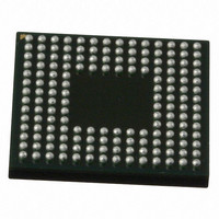
Page 70
... The Package of the PI7C9X7958 is a 160-pin LFBGA. The ball pitch is 0.8mm and the ball size is 0.5mm. The following are the package information and mechanical dimensions. Notes: 1) All dimensions are in millimeters 2) JEDEC# is MO-205F/AE March 2011 – Revision 1.4 Pericom Semiconductor 11-0039 160-Ball Low Profile Fine Pitch Ball Grid Array (LFBGA ...
Page 71
... Order Information Part Number Temperature Range □ -40 PI7C9X7958 NBE (Industrial Temperature 9X7958 NB E March 2011 – Revision 1.4 Pericom Semiconductor 11-0039 Package 160-pin LFBGA 12mm x 12mm Blank=Standar d E=Pb-Fr ee and Gr een Pac kage Code Blank=Standar d =Revision Device Type Device Number Family PI=Per ic om ...