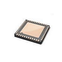
PTN3360DBS,518 NXP Semiconductors, PTN3360DBS,518 Datasheet - Page 10

PTN3360DBS,518
Manufacturer Part Number
PTN3360DBS,518
Description
IC DVI/HDMI LVL SHIFTER 48HVQFN
Manufacturer
NXP Semiconductors
Type
Level Shifterr
Datasheet
1.PTN3360DBS518.pdf
(25 pages)
Specifications of PTN3360DBS,518
Package / Case
48-VFQFN Exposed Pad
Applications
DisplayPort to HDMI, DVI Adapters
Interface
DVI, HDMI
Voltage - Supply
2.85 V ~ 3.6 V
Mounting Type
Surface Mount
Maximum Operating Temperature
+ 85 C
Minimum Operating Temperature
- 40 C
Mounting Style
SMD/SMT
Lead Free Status / RoHS Status
Lead free / RoHS Compliant
Lead Free Status / RoHS Status
Lead free / RoHS Compliant, Lead free / RoHS Compliant
Other names
568-5120-2
Available stocks
Company
Part Number
Manufacturer
Quantity
Price
Company:
Part Number:
PTN3360DBS,518
Manufacturer:
LT
Quantity:
89
NXP Semiconductors
7. Functional description
PTN3360D
Product data sheet
Table 3.
[1]
Refer to
The PTN3360D level shifts four lanes of low-swing AC-coupled differential input signals to
DVI and HDMI compliant open-drain current-steering differential output signals, up to
2.5 Gbit/s per lane to support 36-bit deep color mode. It has integrated 50 Ω termination
resistors for AC-coupled differential input signals. An enable signal OE_N can be used to
turn off the TMDS inputs and outputs, thereby minimizing power consumption. The TMDS
outputs are back-power safe to disallow current flow from a powered sink while the
PTN3360D is unpowered.
The PTN3360D's DDC channel provides active level shifting and buffering, allowing 3.3 V
source-side termination and 5 V sink-side termination. The sink-side DDC ports are
equipped with a rise time accelerator enabling drive of long cables or high bus
capacitance. This enables the system designer to isolate bus capacitance to meet HDMI
DDC version 1.3a distance specification. The PTN3360D offers back-power safe sink-side
I/Os to disallow backdrive current from the DDC clock and data lines when power is off or
when DDC is not enabled. An enable signal DCC_EN enables the DDC level shifter block.
The PTN3360D also provides voltage translation for the Hot Plug Detect (HPD) signal
from 0 V to 5 V on the sink side to 0 V to 3.3 V on the source side.
The PTN3360D does not re-time any data. It contains no state machines. No inputs or
outputs of the device are latched or clocked. Because the PTN3360D acts as a
transparent level shifter, no reset is required.
Symbol
Feature control signals
REXT
n.c.
n.c.
EQ5
HVQFN48 package supply ground is connected to both GND pins and exposed center pad. GND pins and
the exposed center pad must be connected to supply ground for proper device operation. For enhanced
thermal, electrical, and board level performance, the exposed pad needs to be soldered to the board using
a corresponding thermal pad on the board and for proper heat conduction through the board, thermal vias
need to be incorporated in the PCB in the thermal pad region.
Figure 2 “Functional diagram of
Pin description
All information provided in this document is subject to legal disclaimers.
Pin
6
6
4, 10,
34, 35
3
Rev. 2 — 19 November 2010
3.3 V low-voltage
Type
analog I/O
-
-
CMOS quinary input
…continued
HDMI/DVI level shifter supporting deep color mode
PTN3360D”.
Description
(PTN3360DBS only.) Current sense port used to
provide an accurate current reference for the
differential outputs OUT_Dx. For best output
voltage swing accuracy, use of a 10 kΩ resistor
(1 % tolerance) from this terminal to GND is
recommended. May also be tied to either V
GND directly (0 Ω). See
(PTN3360DBS/S900 only.) not connected
not connected
Equalizer setting input pin. This pin can be
board-strapped to one of five decode values:
short to GND, resistor to GND, open-circuit,
resistor to V
truth table.
DD
, short to V
Section 7.2
PTN3360D
DD
. See
© NXP B.V. 2010. All rights reserved.
Table 5
for details.
for
10 of 25
DD
or


