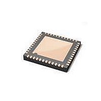
PTN3360DBS,518 NXP Semiconductors, PTN3360DBS,518 Datasheet - Page 13

PTN3360DBS,518
Manufacturer Part Number
PTN3360DBS,518
Description
IC DVI/HDMI LVL SHIFTER 48HVQFN
Manufacturer
NXP Semiconductors
Type
Level Shifterr
Datasheet
1.PTN3360DBS518.pdf
(25 pages)
Specifications of PTN3360DBS,518
Package / Case
48-VFQFN Exposed Pad
Applications
DisplayPort to HDMI, DVI Adapters
Interface
DVI, HDMI
Voltage - Supply
2.85 V ~ 3.6 V
Mounting Type
Surface Mount
Maximum Operating Temperature
+ 85 C
Minimum Operating Temperature
- 40 C
Mounting Style
SMD/SMT
Lead Free Status / RoHS Status
Lead free / RoHS Compliant
Lead Free Status / RoHS Status
Lead free / RoHS Compliant, Lead free / RoHS Compliant
Other names
568-5120-2
Available stocks
Company
Part Number
Manufacturer
Quantity
Price
Company:
Part Number:
PTN3360DBS,518
Manufacturer:
LT
Quantity:
89
NXP Semiconductors
PTN3360D
Product data sheet
7.2 Analog current reference (PTN3360DBS only)
7.3 Equalizer
7.4 Backdrive current protection
7.5 Active DDC buffer with rise time accelerator
The REXT pin (pin 6) is an analog current sense port used to provide an accurate current
reference for the differential outputs OUT_Dx. For best output voltage swing accuracy,
use of a 10 kΩ resistor (1 % tolerance) connected between this terminal and GND is
recommended.
If an external 10 kΩ ± 1 % resistor is not used, this pin can be connected to GND or V
directly (0 Ω). In any of these cases, the output will function normally but at reduced
accuracy over voltage and temperature of the following parameters: output levels (V
differential output voltage swing, and rise and fall time accuracy.
Remark: In PTN3360DBS/S900, pin 6 is not connected (n.c.).
The PTN3360D supports 5 level equalization setting by the quinary input pin EQ5.
Table 5.
The PTN3360D is designed for backdrive prevention on all sink-side TMDS outputs,
sink-side DDC I/Os and the HPD_SINK input. This supports user scenarios where the
display is connected and powered, but the PTN3360D is unpowered. In these cases, the
PTN3360D will sink no more than a negligible amount of leakage current, and will block
the display (sink) termination network from driving the power supply of the PTN3360D or
that of the inactive DVI or HDMI source.
The PTN3360D DDC channel, besides providing 3.3 V to 5 V level shifting, includes
active buffering and rise time acceleration which allows up to 18 meters bus extension for
reliable DDC applications. While retaining all the operating modes and features of the
I
bidirectional buffering for both the data (SDA) and the clock (SCL) line as well as the
rise time accelerator on the sink-side port (SCL_SINK and SDA_SINK) enabling the bus
to drive a load up to 1400 pF or distance of 18 m on the sink-side port, and 400 pF on the
source-side port (SCL_SOURCE and SCA_SOURCE). Using the PTN3360D for DVI or
HDMI level shifting enables the system designer to isolate bus capacitance to meet HDMI
DDC version 1.3 distance specification. The SDA and SCL pins are overvoltage tolerant
and are high-impedance when the PTN3360D is unpowered or when DDC_EN is LOW.
Inputs
EQ5
short to GND
10 kΩ resistor to GND
open-circuit
10 kΩ resistor to V
short to V
2
C-bus system during the level shifts, it permits extension of the I
DD
Equalizer settings
All information provided in this document is subject to legal disclaimers.
DD
Rev. 2 — 19 November 2010
Quinary notation
0
1
2
3
4
5
5
5
5
5
HDMI/DVI level shifter supporting deep color mode
Equalizer mode
0 dB
2 dB
3.5 dB
9 dB
7 dB
2
C-bus by providing
PTN3360D
© NXP B.V. 2010. All rights reserved.
13 of 25
OL
DD
),


