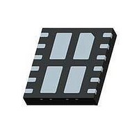
FDMQ8203 Fairchild Semiconductor, FDMQ8203 Datasheet - Page 3

FDMQ8203
Manufacturer Part Number
FDMQ8203
Description
MOSFET Power Dual PT5 N-Ch & Dual PT1 PCH PowerTrench
Manufacturer
Fairchild Semiconductor
Datasheet
1.FDMQ8203.pdf
(10 pages)
Specifications of FDMQ8203
Configuration
Dual
Transistor Polarity
N and P-Channel
Resistance Drain-source Rds (on)
85 mOhms, 161 mOhms
Forward Transconductance Gfs (max / Min)
6 S
Drain-source Breakdown Voltage
100 V, - 80 V
Gate-source Breakdown Voltage
20 V
Continuous Drain Current
3.4 A, - 2.6 A
Power Dissipation
2.5 W
Maximum Operating Temperature
+ 125 C
Mounting Style
SMD/SMT
Package / Case
MLP
Fall Time
1.9 ns, 2.7 ns
Gate Charge Qg
2.9 nC, 13 nC
Rise Time
1.3 ns, 2.8 ns
Lead Free Status / Rohs Status
Details
©2011 Fairchild Semiconductor Corporation
FDMQ8203 Rev.C1
Electrical Characteristics
Drain-Source Diode Characteristics
Notes:
1: R
2: Pulse Test: Pulse Width < 300 μs, Duty cycle < 2.0%.
V
t
Q
rr
SD
rr
by the user's board design.
Symbol
θJA
is determined with the device mounted on a 1 in
Source to Drain Diode Forward Voltage
Reverse Recovery Time
Reverse Recovery Charge
Parameter
a.
50 °C/W when mounted on a 1 in
pad of 2 oz copper, the board
designed Q1+Q3 or Q2+Q4.
T
2
J
pad 2 oz copper pad on a 1.5 x 1.5 in. board of FR-4 material. R
= 25 °C unless otherwise noted
V
V
Q1/Q4:
I
Q2/Q3:
I
F
F
GS
GS
= 3 A, di/dt = 100 A/μs
= -2.3 A, di/dt = 100 A/μs
= 0 V, I
= 0 V, I
2
Test Conditions
3
S
S
= 3 A
= -2.3 A
(Note 2)
(Note 2)
b.
160 °C/W when mounted on
minimum pad of 2 oz copper, the
board designed Q1+Q3 or Q2+Q4.
Q1/Q4
Q2/Q3
Q1/Q4
Q2/Q3
Q1/Q4
Q2/Q3
Type
θJC
is guaranteed by design while R
Min
-0.82
Typ
0.86
32
26
21
26
a
www.fairchildsemi.com
Max
-1.3
1.3
52
42
34
42
θCA
is determined
Units
nC
ns
V


