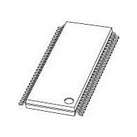
PCF8576DT NXP Semiconductors, PCF8576DT Datasheet - Page 16

PCF8576DT
Manufacturer Part Number
PCF8576DT
Description
Manufacturer
NXP Semiconductors
Datasheet
1.PCF8576DT.pdf
(52 pages)
Specifications of PCF8576DT
Operating Supply Voltage (typ)
2.5/3.3/5V
Number Of Digits
20
Number Of Segments
160
Package Type
TSSOP
Pin Count
56
Mounting
Surface Mount
Power Dissipation
400mW
Frequency (max)
400KHz
Operating Supply Voltage (min)
1.8V
Operating Supply Voltage (max)
5.5V
Lead Free Status / Rohs Status
Supplier Unconfirmed
Available stocks
Company
Part Number
Manufacturer
Quantity
Price
Part Number:
PCF8576DT
Manufacturer:
NXP/恩智浦
Quantity:
20 000
Part Number:
PCF8576DT/2
Manufacturer:
NXP/恩智浦
Quantity:
20 000
NXP Semiconductors
PCF8576D_9
Product data sheet
7.5.1 Internal clock
7.5.2 External clock
7.5 Oscillator
7.6 Timing
7.7 Display register
7.8 Segment outputs
7.9 Backplane outputs
The internal logic of the PCF8576D and its LCD drive signals are timed either by its
internal oscillator or by an external clock. The internal oscillator is enabled by connecting
pin OSC to pin V
as the clock signal for several PCF8576Ds in the system that are connected in cascade.
After power-on, pin SDA must be HIGH to guarantee that the clock starts.
Pin CLK is enabled as an external clock input by connecting pin OSC to V
The LCD frame signal frequency is determined by the clock frequency (f
Remark: A clock signal must always be supplied to the device; removing the clock may
freeze the LCD in a DC state, which is not suitable for the liquid crystal.
The PCF8576D timing controls the internal data flow of the device. This includes the
transfer of display data from the display RAM to the display segment outputs. In cascaded
applications, the correct timing relationship between each PCF8576D in the system is
maintained by the synchronization signal at pin SYNC. The timing also generates the LCD
frame signal whose frequency is derived from the clock frequency. The frame signal
frequency is a fixed division of the clock frequency from either the internal or an external
clock:
The display latch holds the display data while the corresponding multiplex signals are
generated. There is a one-to-one relationship between the data in the display latch, the
LCD segment outputs and each column of the display RAM.
The LCD drive section includes 40 segment outputs S0 to S39 which should be
connected directly to the LCD. The segment output signals are generated in accordance
with the multiplexed backplane signals and with data residing in the display latch. When
less than 40 segment outputs are required, the unused segment outputs should be left
open-circuit.
The LCD drive section includes four backplane outputs BP0 to BP3 which must be
connected directly to the LCD. The backplane output signals are generated in accordance
with the selected LCD drive mode. If less than four backplane outputs are required, the
unused outputs can be left open-circuit.
In the 1:3 multiplex drive mode, BP3 carries the same signal as BP1, therefore these two
adjacent outputs can be tied together to give enhanced drive capabilities.
f
fr
=
f
------- -
24
clk
SS
.
. If the internal oscillator is used, the output from pin CLK can be used
Rev. 09 — 25 August 2009
Universal LCD driver for low multiplex rates
PCF8576D
© NXP B.V. 2009. All rights reserved.
clk
DD
).
.
16 of 52


