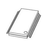
PCF8562TT NXP Semiconductors, PCF8562TT Datasheet - Page 18

PCF8562TT
Manufacturer Part Number
PCF8562TT
Description
Manufacturer
NXP Semiconductors
Datasheet
1.PCF8562TT.pdf
(36 pages)
Specifications of PCF8562TT
Operating Supply Voltage (typ)
2.5/3.3/5V
Number Of Digits
16
Number Of Segments
128
Operating Temperature (min)
-40C
Operating Temperature (max)
85C
Operating Temperature Classification
Industrial
Package Type
TSSOP
Pin Count
48
Mounting
Surface Mount
Power Dissipation
400mW
Frequency (max)
400KHz
Operating Supply Voltage (min)
1.8V
Operating Supply Voltage (max)
5.5V
Lead Free Status / Rohs Status
Compliant
Available stocks
Company
Part Number
Manufacturer
Quantity
Price
Part Number:
PCF8562TT
Manufacturer:
NXP/恩智浦
Quantity:
20 000
Company:
Part Number:
PCF8562TT/2
Manufacturer:
NXP Semiconductors
Quantity:
36 137
Company:
Part Number:
PCF8562TT/2
Manufacturer:
NXP
Quantity:
12 000
Part Number:
PCF8562TT/2
Manufacturer:
NXP/恩智浦
Quantity:
20 000
Company:
Part Number:
PCF8562TT/2Ј¬118
Manufacturer:
NXP
Quantity:
64 000
NXP Semiconductors
7. Characteristics of the I
PCF8562_2
Product data sheet
6.15 Blinker
The PCF8562 has a very versatile display blinking capability. The whole display can blink
at a frequency selected by the Blink command. Each blink frequency is a multiple integer
value of the clock frequency; the ratio between the clock frequency and blink frequency
depends on the blink mode selected, as shown in
Table 5.
[1]
An additional feature allows an arbitrary selection of LCD segments to be blinked in the
static and 1 : 2 drive modes. This is implemented without any communication overheads
by the output bank selector which alternates the displayed data between the data in the
display RAM bank and the data in an alternative RAM bank at the blink frequency. This
mode can also be implemented by the Blink command.
In the 1 : 3 and 1 : 4 drive modes, where no alternative RAM bank is available, groups of
LCD segments can be blinked by selectively changing the display RAM data at fixed time
intervals.
The entire display can be blinked at a frequency other than the nominal blink frequency by
sequentially resetting and setting the display enable bit E at the required rate using the
Mode Set command.
The I
The two lines are a Serial Data Line (SDA) and a Serial Clock Line (SCL). Both lines must
be connected to a positive supply via a pull-up resistor when connected to the output
stages of a device. Data transfer may be initiated only when the bus is not busy.
In chip-on-glass applications where the track resistance from the SDA pad to the system
SDA line can be significant, a potential divider is generated by the bus pull-up resistor and
the Indium Tin Oxide (ITO) track resistance. It is therefore necessary to minimize the track
resistance from the SDA pad to the system SDA line to guarantee a valid LOW-level
during the acknowledge cycle.
Blink mode
Off
2 Hz
1 Hz
0.5 Hz
Blink modes 0.5 Hz, 1 Hz and 2 Hz, and nominal blink frequencies 0.5 Hz, 1 Hz and 2 Hz correspond to an
oscillator frequency (f
[1]
[1]
2
C-bus is for bidirectional, two-line communication between different ICs or modules.
[1]
Blinking frequencies
2
C-bus
CLK
Rev. 02 — 22 January 2007
) of 1536 Hz at pin CLK. The oscillator frequency range is given in
Normal operating mode ratio Nominal blink frequency
-
------------ -
------------ -
------------ -
1536
3072
f
f
f
768
CLK
CLK
CLK
Universal LCD driver for low multiplex rates
Table
5.
blinking off
2 Hz
1 Hz
0.5 Hz
[1]
[1]
[1]
PCF8562
© NXP B.V. 2007. All rights reserved.
Section
18 of 36
11.


