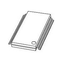
PCF8562TT NXP Semiconductors, PCF8562TT Datasheet - Page 28

PCF8562TT
Manufacturer Part Number
PCF8562TT
Description
Manufacturer
NXP Semiconductors
Datasheet
1.PCF8562TT.pdf
(36 pages)
Specifications of PCF8562TT
Operating Supply Voltage (typ)
2.5/3.3/5V
Number Of Digits
16
Number Of Segments
128
Operating Temperature (min)
-40C
Operating Temperature (max)
85C
Operating Temperature Classification
Industrial
Package Type
TSSOP
Pin Count
48
Mounting
Surface Mount
Power Dissipation
400mW
Frequency (max)
400KHz
Operating Supply Voltage (min)
1.8V
Operating Supply Voltage (max)
5.5V
Lead Free Status / Rohs Status
Compliant
Available stocks
Company
Part Number
Manufacturer
Quantity
Price
Part Number:
PCF8562TT
Manufacturer:
NXP/恩智浦
Quantity:
20 000
Company:
Part Number:
PCF8562TT/2
Manufacturer:
NXP Semiconductors
Quantity:
36 137
Company:
Part Number:
PCF8562TT/2
Manufacturer:
NXP
Quantity:
12 000
Part Number:
PCF8562TT/2
Manufacturer:
NXP/恩智浦
Quantity:
20 000
Company:
Part Number:
PCF8562TT/2Ј¬118
Manufacturer:
NXP
Quantity:
64 000
NXP Semiconductors
11. Dynamic characteristics
Table 19.
V
[1]
[2]
[3]
PCF8562_2
Product data sheet
Symbol
f
t
t
t
t
t
Timing characteristics: I
f
t
t
t
t
t
t
t
C
t
t
t
t
CLK
CLKH
CLKL
PD(SYNC)
SYNCL
PD(LCD)
SCL
BUF
HD;STA
SU;STA
LOW
HIGH
r
f
SU;DAT
HD;DAT
SU;STO
SP
DD
b
= 1.8 V to 5.5 V; V
Typical output duty factor: 50 % measured at the CLK output pin.
Not tested in production.
All timing values are valid within the operating supply voltage and ambient temperature range and are referenced to V
input voltage swing of V
Dynamic characteristics
Parameter
oscillator frequency
input CLK HIGH time
input CLK LOW time
SYNC propagation delay
SYNC LOW time
driver delays with test loads
SCL clock frequency
bus free time between a STOP and START
START condition hold time
set-up time for a repeated START condition
SCL LOW time
SCL HIGH time
SCL and SDA rise time
SCL and SDA fall time
capacitive load for each bus line
data set-up time
data hold time
set-up time for STOP condition
pulse width of spikes that must be suppressed by
the input filter
SS
SS
= 0 V; V
2
Fig 18. Test loads
C-bus
to V
DD
[3]
LCD
.
= 2.5 V to 6.5 V; T
BP0 to BP3, and
S0 to S31
Rev. 02 — 22 January 2007
SYNC
CLK
amb
= 40 C to +85 C; unless otherwise specified.
3.3 k
6.8
(2 %)
(2 %)
1 nF
Conditions
V
f
f
SCL
SCL
LCD
V
0.5V
V
= 400 kHz
< 400 kHz
DD
SS
Universal LCD driver for low multiplex rates
= 5 V
DD
SDA,
SCL
[1]
[2]
Min
960
60
60
-
1
-
-
1.3
0.6
0.6
1.3
0.6
-
-
-
-
100
0
0.6
-
1.5 k
(2 %)
001aac267
Typ
1890
-
-
30
-
-
-
-
-
-
-
-
-
-
-
-
-
-
-
-
V
PCF8562
DD
© NXP B.V. 2007. All rights reserved.
IL
Max
2640
-
-
-
-
30
400
-
-
-
-
-
0.3
1.0
0.3
400
-
-
-
50
and V
IH
28 of 36
Unit
Hz
ns
kHz
pF
ns
ns
ns
with an
s
s
s
s
s
s
s
s
s
s
s
s
s


