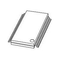
PCF8562TT NXP Semiconductors, PCF8562TT Datasheet - Page 21

PCF8562TT
Manufacturer Part Number
PCF8562TT
Description
Manufacturer
NXP Semiconductors
Datasheet
1.PCF8562TT.pdf
(36 pages)
Specifications of PCF8562TT
Operating Supply Voltage (typ)
2.5/3.3/5V
Number Of Digits
16
Number Of Segments
128
Operating Temperature (min)
-40C
Operating Temperature (max)
85C
Operating Temperature Classification
Industrial
Package Type
TSSOP
Pin Count
48
Mounting
Surface Mount
Power Dissipation
400mW
Frequency (max)
400KHz
Operating Supply Voltage (min)
1.8V
Operating Supply Voltage (max)
5.5V
Lead Free Status / Rohs Status
Compliant
Available stocks
Company
Part Number
Manufacturer
Quantity
Price
Part Number:
PCF8562TT
Manufacturer:
NXP/恩智浦
Quantity:
20 000
Company:
Part Number:
PCF8562TT/2
Manufacturer:
NXP Semiconductors
Quantity:
36 137
Company:
Part Number:
PCF8562TT/2
Manufacturer:
NXP
Quantity:
12 000
Part Number:
PCF8562TT/2
Manufacturer:
NXP/恩智浦
Quantity:
20 000
Company:
Part Number:
PCF8562TT/2Ј¬118
Manufacturer:
NXP
Quantity:
64 000
NXP Semiconductors
PCF8562_2
Product data sheet
7.7 I
Two I
The least significant bit of the slave address that a PCF8562 will respond to is defined by
the level tied to its SA0 input. The PCF8562 is a write-only device and will not respond to
a read access.
The I
condition (S) from the I
slave addresses available. All PCF8562s whose SA0 inputs correspond to bit 0 of the
slave address respond by asserting an acknowledge in parallel. This I
ignored by all PCF8562s whose SA0 inputs are set to the alternative level.
After an acknowledgement, one or more command bytes follow which define the status of
the PCF8562.
The last command byte sent is identified by resetting its most significant bit, continuation
bit C, (see
PCF8562s on the bus.
After the last command byte, one or more display data bytes may follow. Display data
bytes are stored in the display RAM at the address specified by the data pointer and the
subaddress counter. Both data pointer and subaddress counter are automatically
updated.
An acknowledgement after each byte is asserted only by PCF8562s that are addressed
via address lines A0, A1 and A2. After the last display byte, the I
Stop condition (P). Alternately a Start may be asserted to Restart an I
2
Fig 15. I
Fig 16. Format of command byte
C-bus protocol
2
2
C-bus protocol is shown in
C-bus slave addresses (01110000 and 01110010) are reserved for the PCF8562.
C = 0 = last command.
C = 1 = commands continue.
2
C-bus protocol
S
Figure
0 1 1 1 0 0
slave address
16). The command bytes are also acknowledged by all addressed
1 byte
Rev. 02 — 22 January 2007
2
C-bus master which is followed by one of two possible PCF8562
S
A
0
R/W
MSB
0 A C
C
Figure
acknowledge
n
COMMAND
REST OF OPCODE
1 byte(s)
15. The sequence is initiated with a Start
Universal LCD driver for low multiplex rates
A
msa833
DISPLAY DATA
n
LSB
0 byte(s)
2
C-bus master asserts a
update data pointers
acknowledge
2
2
PCF8562
C-bus transfer is
C-bus access.
© NXP B.V. 2007. All rights reserved.
A
001aac266
P
21 of 36


