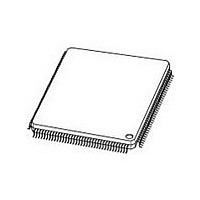
LPC2214FBD144 NXP Semiconductors, LPC2214FBD144 Datasheet - Page 22

LPC2214FBD144
Manufacturer Part Number
LPC2214FBD144
Description
Manufacturer
NXP Semiconductors
Datasheet
1.LPC2214FBD144.pdf
(45 pages)
Specifications of LPC2214FBD144
Cpu Family
LPC2000
Device Core
ARM7TDMI-S
Device Core Size
16/32Bit
Frequency (max)
60MHz
Interface Type
I2C/SPI
Program Memory Type
Flash
Program Memory Size
256KB
Total Internal Ram Size
16KB
# I/os (max)
112
Number Of Timers - General Purpose
2
Operating Supply Voltage (typ)
1.8/3.3V
Operating Supply Voltage (max)
1.95/3.6V
Operating Supply Voltage (min)
1.65/2.5/3V
On-chip Adc
8-chx10-bit
Instruction Set Architecture
RISC
Operating Temp Range
-40C to 85C
Operating Temperature Classification
Industrial
Mounting
Surface Mount
Pin Count
144
Package Type
LQFP
Lead Free Status / Rohs Status
Compliant
Available stocks
Company
Part Number
Manufacturer
Quantity
Price
Part Number:
LPC2214FBD144
Manufacturer:
NXP
Quantity:
20 000
Company:
Part Number:
LPC2214FBD144,551
Manufacturer:
NXP Semiconductors
Quantity:
10 000
Company:
Part Number:
LPC2214FBD144/01
Manufacturer:
LT
Quantity:
3 400
Company:
Part Number:
LPC2214FBD144/01
Manufacturer:
NXP
Quantity:
5 000
Part Number:
LPC2214FBD144/01
Manufacturer:
NXP/恩智浦
Quantity:
20 000
Company:
Part Number:
LPC2214FBD144/01,5
Manufacturer:
Intersil
Quantity:
637
Company:
Part Number:
LPC2214FBD144/01,5
Manufacturer:
NXP Semiconductors
Quantity:
10 000
Part Number:
LPC2214FBD144/01,5
Manufacturer:
NXP/恩智浦
Quantity:
20 000
Company:
Part Number:
LPC2214FBD144/015
Manufacturer:
NXP Semiconductors
Quantity:
135
NXP Semiconductors
LPC2212_2214_4
Product data sheet
6.18.1 Crystal oscillator
6.18.2 PLL
6.18.3 Reset and wake-up timer
6.18 System control
The oscillator supports crystals in the range of 1 MHz to 30 MHz. The oscillator output
frequency is called f
purposes of rate equations, etc. f
running and connected. Refer to
The PLL accepts an input clock frequency in the range of 10 MHz to 25 MHz. The input
frequency is multiplied up into the range of 10 MHz to 60 MHz with a Current Controlled
Oscillator (CCO). The multiplier can be an integer value from 1 to 32 (in practice, the
multiplier value cannot be higher than 6 on this family of microcontrollers due to the upper
frequency limit of the CPU). The CCO operates in the range of 156 MHz to 320 MHz, so
there is an additional divider in the loop to keep the CCO within its frequency range while
the PLL is providing the desired output frequency. The output divider may be set to divide
by 2, 4, 8, or 16 to produce the output clock. Since the minimum output divider value is 2,
it is insured that the PLL output has a 50 % duty cycle. The PLL is turned off and
bypassed following a chip Reset and may be enabled by software. The program must
configure and activate the PLL, wait for the PLL to Lock, then connect to the PLL as a
clock source. The PLL settling time is 100 s.
Reset has two sources on the LPC2212/2214: the RESET pin and Watchdog Reset. The
RESET pin is a Schmitt trigger input pin with an additional glitch filter. Assertion of chip
Reset by any source starts the Wake-up Timer (see Wake-up Timer description below),
causing the internal chip reset to remain asserted until the external Reset is de-asserted,
the oscillator is running, a fixed number of clocks have passed, and the on-chip flash
controller has completed its initialization.
When the internal Reset is removed, the processor begins executing at address 0, which
is the Reset vector. At that point, all of the processor and peripheral registers have been
initialized to predetermined values.
The Wake-up Timer ensures that the oscillator and other analog functions required for
chip operation are fully functional before the processor is allowed to execute instructions.
This is important at power on, all types of Reset, and whenever any of the aforementioned
•
•
•
•
•
Pulse period and width can be any number of timer counts. This allows complete
flexibility in the trade-off between resolution and repetition rate. All PWM outputs will
occur at the same repetition rate.
Double edge controlled PWM outputs can be programmed to be either positive going
or negative going pulses.
Match register updates are synchronized with pulse outputs to prevent generation of
erroneous pulses. Software must ‘release’ new match values before they can become
effective.
May be used as a standard timer if the PWM mode is not enabled.
A 32-bit Timer/Counter with a programmable 32-bit Prescaler.
osc
Rev. 04 — 3 January 2008
and the ARM processor clock frequency is referred to as CCLK for
Section 6.18.2 “PLL”
osc
and CCLK are the same value unless the PLL is
for additional information.
16/32-bit ARM microcontrollers
LPC2212/2214
© NXP B.V. 2008. All rights reserved.
22 of 45


