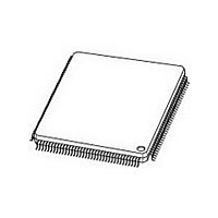
LPC2214FBD144 NXP Semiconductors, LPC2214FBD144 Datasheet - Page 8

LPC2214FBD144
Manufacturer Part Number
LPC2214FBD144
Description
Manufacturer
NXP Semiconductors
Datasheet
1.LPC2214FBD144.pdf
(45 pages)
Specifications of LPC2214FBD144
Cpu Family
LPC2000
Device Core
ARM7TDMI-S
Device Core Size
16/32Bit
Frequency (max)
60MHz
Interface Type
I2C/SPI
Program Memory Type
Flash
Program Memory Size
256KB
Total Internal Ram Size
16KB
# I/os (max)
112
Number Of Timers - General Purpose
2
Operating Supply Voltage (typ)
1.8/3.3V
Operating Supply Voltage (max)
1.95/3.6V
Operating Supply Voltage (min)
1.65/2.5/3V
On-chip Adc
8-chx10-bit
Instruction Set Architecture
RISC
Operating Temp Range
-40C to 85C
Operating Temperature Classification
Industrial
Mounting
Surface Mount
Pin Count
144
Package Type
LQFP
Lead Free Status / Rohs Status
Compliant
Available stocks
Company
Part Number
Manufacturer
Quantity
Price
Part Number:
LPC2214FBD144
Manufacturer:
NXP
Quantity:
20 000
Company:
Part Number:
LPC2214FBD144,551
Manufacturer:
NXP Semiconductors
Quantity:
10 000
Company:
Part Number:
LPC2214FBD144/01
Manufacturer:
LT
Quantity:
3 400
Company:
Part Number:
LPC2214FBD144/01
Manufacturer:
NXP
Quantity:
5 000
Part Number:
LPC2214FBD144/01
Manufacturer:
NXP/恩智浦
Quantity:
20 000
Company:
Part Number:
LPC2214FBD144/01,5
Manufacturer:
Intersil
Quantity:
637
Company:
Part Number:
LPC2214FBD144/01,5
Manufacturer:
NXP Semiconductors
Quantity:
10 000
Part Number:
LPC2214FBD144/01,5
Manufacturer:
NXP/恩智浦
Quantity:
20 000
Company:
Part Number:
LPC2214FBD144/015
Manufacturer:
NXP Semiconductors
Quantity:
135
NXP Semiconductors
Table 3.
LPC2212_2214_4
Product data sheet
Symbol
P0[30]/AIN3/EINT3/
CAP0[0]
P1[0] to P1[31]
P1[0]/CS0
P1[1]/OE
P1[16]/TRACEPKT0
P1[17]/TRACEPKT1
P1[18]/TRACEPKT2
P1[19]/TRACEPKT3
P1[20]/TRACESYNC
P1[21]/PIPESTAT0
P1[22]/PIPESTAT1
P1[23]/PIPESTAT2
P1[24]/TRACECLK
P1[25]/EXTIN0
P1[26]/RTCK
P1[27]/TDO
P1[28]/TDI
P1[29]/TCK
P1[30]/TMS
P1[31]/TRST
P2[0] to P2[31]
P2[0]/D0
P2[1]/D1
P2[2]/D2
P2[3]/D3
P2[4]/D4
P2[5]/D5
P2[6]/D6
Pin description
Pin
33
91
90
34
24
15
7
102
95
86
82
70
60
52
144
140
126
113
43
98
105
106
108
109
114
115
…continued
Type Description
I
I
I
I/O
O
O
O
O
O
O
O
O
O
O
O
I
I/O
O
I
I
I
I
I/O
I/O
I/O
I/O
I/O
I/O
I/O
I/O
AIN3 — ADC, input 3. This analog input is always connected to its pin.
EINT3 — External interrupt 3 input.
CAP0[0] — Capture input for Timer 0, channel 0.
Port 1 is a 32-bit bidirectional I/O port with individual direction controls for
each bit. The operation of port 1 pins depends upon the pin function selected
via the Pin Connect Block.
Pins 2 through 15 of port 1 are not available.
LOW-active Chip Select 0 signal.
(Bank 0 addresses range 0x8000 0000 to 0x80FF FFFF)
LOW-active Output Enable signal.
Trace Packet, bit 0. Standard I/O port with internal pull-up.
Trace Packet, bit 1. Standard I/O port with internal pull-up.
Trace Packet, bit 2. Standard I/O port with internal pull-up.
Trace Packet, bit 3. Standard I/O port with internal pull-up.
Trace Synchronization; standard I/O port with internal pull-up.
Note: LOW on this pin while RESET is LOW, enables pins P1[25:16] to
operate as Trace port after reset.
Pipeline Status, bit 0. Standard I/O port with internal pull-up.
Pipeline Status, bit 1. Standard I/O port with internal pull-up.
Pipeline Status, bit 2. Standard I/O port with internal pull-up.
Trace Clock. Standard I/O port with internal pull-up.
External Trigger Input. Standard I/O with internal pull-up.
Returned Test Clock output. Extra signal added to the JTAG port. Assists
debugger synchronization when processor frequency varies. Bidirectional pin
with internal pull-up.
Note: LOW on this pin while RESET is LOW, enables pins P1[31:26] to
operate as Debug port after reset.
Test Data out for JTAG interface.
Test Data in for JTAG interface.
Test Clock for JTAG interface. This clock must be slower than
clock (CCLK) for the JTAG interface to operate.
Test Mode Select for JTAG interface.
Test Reset for JTAG interface.
Port 2 is a 32-bit bidirectional I/O port with individual direction controls for
each bit. The operation of port 2 pins depends upon the pin function selected
via the Pin Connect Block.
External memory data line 0.
External memory data line 1.
External memory data line 2.
External memory data line 3.
External memory data line 4.
External memory data line 5.
External memory data line 6.
Rev. 04 — 3 January 2008
16/32-bit ARM microcontrollers
LPC2212/2214
© NXP B.V. 2008. All rights reserved.
1
6
of the CPU
8 of 45


