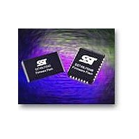
SST49LF004B-33-4C-NH Microchip Technology, SST49LF004B-33-4C-NH Datasheet - Page 14

SST49LF004B-33-4C-NH
Manufacturer Part Number
SST49LF004B-33-4C-NH
Description
Flash 512K X 8 33ns
Manufacturer
Microchip Technology
Datasheet
1.SST49LF004B-33-4C-NH.pdf
(36 pages)
Specifications of SST49LF004B-33-4C-NH
Data Bus Width
8 bit
Memory Type
NAND
Memory Size
4 Mbit
Architecture
Sectored
Interface Type
LPC
Access Time
33 ns
Supply Voltage (max)
3.6 V
Supply Voltage (min)
3 V
Maximum Operating Current
12 mA
Operating Temperature
+ 70 C
Mounting Style
SMD/SMT
Package / Case
PLCC-32
Organization
512 KB x 8
Lead Free Status / Rohs Status
No
Available stocks
Company
Part Number
Manufacturer
Quantity
Price
Company:
Part Number:
SST49LF004B-33-4C-NH
Manufacturer:
SST
Quantity:
5 530
Company:
Part Number:
SST49LF004B-33-4C-NH
Manufacturer:
SST
Quantity:
5 120
Part Number:
SST49LF004B-33-4C-NH
Manufacturer:
SST
Quantity:
20 000
Company:
Part Number:
SST49LF004B-33-4C-NHE
Manufacturer:
SST
Quantity:
5 530
Company:
Part Number:
SST49LF004B-33-4C-NHE
Manufacturer:
SST
Quantity:
5 120
Company:
Part Number:
SST49LF004B-33-4C-NHE
Manufacturer:
SST
Quantity:
48
Part Number:
SST49LF004B-33-4C-NHE
Manufacturer:
SST
Quantity:
20 000
EOL Data Sheet
Abort Mechanism
If LFRAME# is driven low for one or more clock cycles after
the start of a bus cycle, the cycle will be terminated. The
host may drive LAD[3:0] with '1111b' (ABORT nibble) to
return the interface to ready mode. The ABORT only
affects the current bus cycle. For a multi-cycle command
sequence, such as the Erase or Program SDP commands,
ABORT doesn't interrupt the entire command sequence,
only the current bus cycle of the command sequence. The
host can re-send the bus cycle for the aborted command
and continue the SDP command sequence after the device
is ready again.
Response to Invalid Fields for Firmware
Memory Cycle
During LPC operations the SST49LF004B will not explicitly
indicate that it has received invalid field sequences. The
response to specific invalid fields or sequences is as fol-
lows:
ID mismatch: If the IDSEL field does not match ID[3:0],
the device will ignore the cycle. See Multiple Device Selec-
tion section for details.
Address out of range: The address sequence is 7
fields long (28 bits) for Firmware Memory bus cycles, but
only A
Address A
writes to the flash core (A
(A
Invalid MSIZE field If the device receives an invalid
MSIZE field during a Firmware Memory Read or Write
cycle, the cycle will be ignored and no operation will be
attempted. The SST49LF004B will not generate any kind
of response in this situation. Invalid size fields for a Firm-
ware Memory cycle are any data other than 0000b.
Once valid START, IDSEL, and MSIZE fields are received,
the SST49LF004B will always complete the bus cycle.
However, if the device is busy performing a flash Erase or
Program operation, no new Write command (memory write
or register write) will be executed.
©2007 Silicon Storage Technology, Inc.
22
=0).
22
and A
22
has the special function of directing reads and
18
:A
0
will be decoded by SST49LF004B.
22
=1) or to the register space
14
Multiple Device Selection
Multiple LPC flash devices may be strapped to increase
memory densities in a system. The four ID pins, ID[3:0],
allow up to 16 devices to be attached to the same bus by
using different ID strapping in a system. BIOS support, bus
loading, or the attaching bridge may limit this number. The
boot device must have an ID of 0000b (determined by
ID[3:0]); subsequent devices use incremental numbering.
Equal density must be used with multiple devices.
Multiple Device Selection for
Firmware Memory Cycle
For Firmware Memory Read/Write cycles, hardware strap-
ping values on ID[3:0] must match the values in IDSEL
field. See Table 6 for multiple device selection configura-
tions. The SST49LF004B will compare the IDSEL field with
ID[3:0]'s strapping values. If there is a mismatch, the device
will ignore the reminder of the cycle.
TABLE 6: F
Device #
0 (Boot device)
1
2
3
4
5
6
7
8
9
10
11
12
13
14
15
S
IRMWARE
ELECTION
M
C
4 Mbit Firmware Hub
EMORY
ONFIGURATION
ID[3:0]
0000
0001
0010
0011
0100
0101
0110
0111
1000
1001
1010
1011
1100
1101
1110
1111
M
SST49LF004B
ULTIPLE
S71307-03-EOL
D
IDSEL
EVICE
0000
0001
0010
0011
0100
0101
0110
0111
1000
1001
1010
1011
1100
1101
1110
1111
T6.0 1307
12/07


