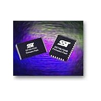
SST49LF004B-33-4C-NH Microchip Technology, SST49LF004B-33-4C-NH Datasheet - Page 17

SST49LF004B-33-4C-NH
Manufacturer Part Number
SST49LF004B-33-4C-NH
Description
Flash 512K X 8 33ns
Manufacturer
Microchip Technology
Datasheet
1.SST49LF004B-33-4C-NH.pdf
(36 pages)
Specifications of SST49LF004B-33-4C-NH
Data Bus Width
8 bit
Memory Type
NAND
Memory Size
4 Mbit
Architecture
Sectored
Interface Type
LPC
Access Time
33 ns
Supply Voltage (max)
3.6 V
Supply Voltage (min)
3 V
Maximum Operating Current
12 mA
Operating Temperature
+ 70 C
Mounting Style
SMD/SMT
Package / Case
PLCC-32
Organization
512 KB x 8
Lead Free Status / Rohs Status
No
Available stocks
Company
Part Number
Manufacturer
Quantity
Price
Company:
Part Number:
SST49LF004B-33-4C-NH
Manufacturer:
SST
Quantity:
5 530
Company:
Part Number:
SST49LF004B-33-4C-NH
Manufacturer:
SST
Quantity:
5 120
Part Number:
SST49LF004B-33-4C-NH
Manufacturer:
SST
Quantity:
20 000
Company:
Part Number:
SST49LF004B-33-4C-NHE
Manufacturer:
SST
Quantity:
5 530
Company:
Part Number:
SST49LF004B-33-4C-NHE
Manufacturer:
SST
Quantity:
5 120
Company:
Part Number:
SST49LF004B-33-4C-NHE
Manufacturer:
SST
Quantity:
48
Part Number:
SST49LF004B-33-4C-NHE
Manufacturer:
SST
Quantity:
20 000
4 Mbit Firmware Hub
SST49LF004B
PARALLEL PROGRAMMING MODE
Device Operation
Commands are used to initiate the memory operation func-
tions of the device. The data portion of the software com-
mand sequence is latched on the rising edge of WE#.
During the software command sequence the row address
is latched on the falling edge of R/C# and the column
address is latched on the rising edge of R/C#.
Read
The Read operation of the SST49LF004B device is con-
trolled by OE#. OE# is the output control and is used to
gate data from the output pins. Refer to the Read cycle tim-
ing diagram, Figure 11, for further details.
Reset
A V
Byte-Program Operation
The SST49LF004B device is programmed on a byte-by-
byte basis. Before programming, one must ensure that the
byte that is being programmed is fully erased. The Byte-
Program operation is initiated by executing a four-byte com-
mand load sequence for Software Data Protection with
address (PA) and data in the last bus cycle. During the
Byte-Program operation, the row address (A
latched on the falling edge of R/C# and the column
Address (A
The data bus is latched on the rising edge of WE#. The
Program operation, once initiated, will be completed, within
20 µs. See Figure 15 for timing waveforms. During the Pro-
gram operation, the only valid reads are Data# Polling and
Toggle Bit. During the internal Program operation, the host
is free to perform additional tasks. Any commands written
during the internal Program operation will be ignored.
Sector-Erase Operation
The Sector-Erase operation allows the system to erase the
device on a sector-by-sector basis. The sector architecture
is based on uniform sector size of 4 KByte. The Sector-
Erase operation is initiated by executing a six-byte com-
mand load sequence for Software Data Protection with
Sector-Erase command (30H) and sector address (SA) in
the last bus cycle. The internal Erase operation begins after
the sixth WE# pulse. The End-of-Erase can be determined
using either Data# Polling or Toggle Bit methods. See Fig-
ure 16 for Sector-Erase timing waveforms. Any commands
written during the Sector-Erase operation will be ignored.
©2007 Silicon Storage Technology, Inc.
IL
on RST# pin initiates a device reset.
21
-A
11
) is latched on the rising edge of R/C#.
10
-A
0
) is
17
Block-Erase Operation
The Block-Erase operation allows the system to erase the
device in any of the 8 uniform 64 KByte blocks for the
SST49LF004B. The Block-Erase operation is initiated by
executing a six-byte command load sequence for Software
Data Protection with Block-Erase command (50H) and
block address (BA) in the last bus cycle. The internal Block-
Erase operation begins after the sixth WE# pulse. The
End-of-Erase can be determined using either Data# Polling
or Toggle Bit methods. See Figure 17 for timing waveforms.
Any commands written during the Block- Erase operation
will be ignored.
Chip-Erase Operation
The SST49LF004B device provides a Chip-Erase opera-
tion only in PP mode, which allows the user to erase the
entire memory array to the '1's state. This is useful when
the entire device must be quickly erased.
The Chip-Erase operation is initiated by executing a six-
byte Software Data Protection command sequence with
Chip-Erase command (10H) with address 5555H in the last
bus cycle. The internal Erase operation begins with the ris-
ing edge of the sixth WE#. During the internal Erase opera-
tion, the only valid reads are Toggle Bit or Data# Polling.
See Table 10 for the command sequence, Figure 18 for
timing diagram. Any commands written during the Chip-
Erase operation will be ignored.
Write Operation Status Detection
The SST49LF004B device provides two software means to
detect the completion of a Write (Program or Erase) cycle,
in order to optimize the system Write cycle time. The soft-
ware detection includes two status bits: Data# Polling DQ
and Toggle Bit DQ
enabled after the rising edge of WE# which initiates the
internal Program or Erase operation.
The actual completion of the nonvolatile write is asynchro-
nous with the system; therefore, either a Data# Polling or
Toggle Bit read may be simultaneous with the completion of
the Write cycle. If this occurs, the system may possibly get
an erroneous result, i.e., valid data may appear to conflict
with either DQ
tion, if an erroneous result occurs, the software routine
should include a loop to read the accessed location an addi-
tional two (2) times. If both reads are valid, the device has
completed the Write cycle, otherwise the rejection is valid.
7
or DQ
6.
The End-of-Write detection mode is
6.
In order to prevent spurious rejec-
S71307-03-EOL
EOL Data Sheet
12/07
7


