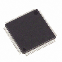
DS21352L+ Maxim Integrated Products, DS21352L+ Datasheet - Page 29

DS21352L+
Manufacturer Part Number
DS21352L+
Description
IC TXRX T1 1-CHIP 3.3V 100-LQFP
Manufacturer
Maxim Integrated Products
Datasheet
1.DS21352L.pdf
(137 pages)
Specifications of DS21352L+
Function
Single-Chip Transceiver
Interface
HDLC, T1
Number Of Circuits
1
Voltage - Supply
3.14 V ~ 3.47 V
Current - Supply
75mA
Operating Temperature
0°C ~ 70°C
Mounting Type
Surface Mount
Package / Case
100-LQFP
Includes
DSX-1 and CSU Line Build-Out Generator, HDLC Controller, In-Band Loop Code Generator and Detector
Lead Free Status / RoHS Status
Lead free / RoHS Compliant
Power (watts)
-
- Current page: 29 of 137
- Download datasheet (2Mb)
NOTES:
1. TEST1, TEST2, TEST3 and TEST4 registers are used by the factory; these registers must be cleared (set to 00h) on power–
up initialization to insure proper operation.
2. Register banks Axh, Bxh, Cxh, Dxh, Exh, and Fxh are not accessible.
3. Upper nibble of the PCVCR1 register is used for MOSCR1
6. CONTROL, ID, AND TEST REGISTERS
The operation of the DS21352/552 is configured via a set of eleven control registers. Typically, the
control registers are only accessed when the system is first powered up. Once the DS21352/552 has been
initialized, the control registers will only need to be accessed when there is a change in the system
configuration. There are two Receive Control Registers (RCR1 and RCR2), two Transmit Control
Registers (TCR1 and TCR2), and seven Common Control Registers (CCR1 to CCR7). Each of the eleven
registers are described in this section.
6.1 POWER-UP SEQUENCE
On power–up, after the supplies are stable the DS21352/552 should be configured for operation by
writing to all of the internal registers (this includes setting the Test Registers to 00h) since the contents of
the internal registers cannot be predicted on power–up. The LIRST (CCR7.7) should be toggled from
zero to one to reset the line interface circuitry (it will take the DS21352/552 about 40ms to recover from
the LIRST bit being toggled). Finally, after the TSYSCLK and RSYSCLK inputs are stable, the ESR bit
should be toggled from a zero to a one (this step can be skipped if the elastic stores are disabled).
6.2 DEVICE ID
There is a device IDentification Register (IDR) at address 0Fh. The MSB of this read–only register is
fixed to a zero indicating that a T1 device is present. The next 3 MSBs are used to indicate which T1
device is present; DS2152, DS21352, or DS21552. The E1 pin–for–pin compatible SCTs will have a
logic one in the MSB position with the following 3 MSBs indicating which E1 SCT is present; DS2154,
DS21354, or DS21554. Table 6-1 represents the possible variations of these bits and the associated SCT.
IDR: DEVICE IDENTIFICATION REGISTER (Address=0F Hex)
SYMBOL
(MSB)
T1E1
T1E1
9A
9B
9C
9D
8F
90
91
92
93
94
95
96
97
98
99
9E
9F
POSITION
Bit 6
R/W
R/W
R/W
R/W
R/W
R/W
R/W
R/W
IDR.7
-
-
-
-
-
-
-
-
-
Receive Channel 16
Receive HDLC DS0 Control Register 1
Receive HDLC DS0 Control Register 2
Transmit HDLC DS0 Control Register 1
Transmit HDLC DS0 Control Register 2
Interleave Bus Operation Register
Test 3 SEE NOTE 1
Test 4 SEE NOTE 1
not present
not present
not present
not present
not present
not present
not present
not present
not present
Bit 5
NAME AND DESCRIPTION
T1 or E1 Chip Determination Bit.
Bit 4
29 of 137
ID3
ID2
TEST3 (set to 00h)
TEST4 (set to 00h)
RDC1
RDC2
TDC1
TDC2
RC16
IBO
-
-
-
-
-
-
-
-
-
ID1
DS21352/DS21552
(LSB)
ID0
Related parts for DS21352L+
Image
Part Number
Description
Manufacturer
Datasheet
Request
R

Part Number:
Description:
MAX7528KCWPMaxim Integrated Products [CMOS Dual 8-Bit Buffered Multiplying DACs]
Manufacturer:
Maxim Integrated Products
Datasheet:

Part Number:
Description:
Single +5V, fully integrated, 1.25Gbps laser diode driver.
Manufacturer:
Maxim Integrated Products
Datasheet:

Part Number:
Description:
Single +5V, fully integrated, 155Mbps laser diode driver.
Manufacturer:
Maxim Integrated Products
Datasheet:

Part Number:
Description:
VRD11/VRD10, K8 Rev F 2/3/4-Phase PWM Controllers with Integrated Dual MOSFET Drivers
Manufacturer:
Maxim Integrated Products
Datasheet:

Part Number:
Description:
Highly Integrated Level 2 SMBus Battery Chargers
Manufacturer:
Maxim Integrated Products
Datasheet:

Part Number:
Description:
Current Monitor and Accumulator with Integrated Sense Resistor; ; Temperature Range: -40°C to +85°C
Manufacturer:
Maxim Integrated Products

Part Number:
Description:
TSSOP 14/A�/RS-485 Transceivers with Integrated 100O/120O Termination Resis
Manufacturer:
Maxim Integrated Products

Part Number:
Description:
TSSOP 14/A�/RS-485 Transceivers with Integrated 100O/120O Termination Resis
Manufacturer:
Maxim Integrated Products

Part Number:
Description:
QFN 16/A�/AC-DC and DC-DC Peak-Current-Mode Converters with Integrated Step
Manufacturer:
Maxim Integrated Products

Part Number:
Description:
TDFN/A/65V, 1A, 600KHZ, SYNCHRONOUS STEP-DOWN REGULATOR WITH INTEGRATED SWI
Manufacturer:
Maxim Integrated Products

Part Number:
Description:
Integrated Temperature Controller f
Manufacturer:
Maxim Integrated Products

Part Number:
Description:
SOT23-6/I�/45MHz to 650MHz, Integrated IF VCOs with Differential Output
Manufacturer:
Maxim Integrated Products

Part Number:
Description:
SOT23-6/I�/45MHz to 650MHz, Integrated IF VCOs with Differential Output
Manufacturer:
Maxim Integrated Products

Part Number:
Description:
EVALUATION KIT/2.4GHZ TO 2.5GHZ 802.11G/B RF TRANSCEIVER WITH INTEGRATED PA
Manufacturer:
Maxim Integrated Products

Part Number:
Description:
QFN/E/DUAL PCIE/SATA HIGH SPEED SWITCH WITH INTEGRATED BIAS RESISTOR
Manufacturer:
Maxim Integrated Products
Datasheet:


