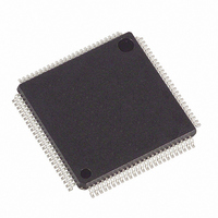
DS21352L+ Maxim Integrated Products, DS21352L+ Datasheet - Page 63

DS21352L+
Manufacturer Part Number
DS21352L+
Description
IC TXRX T1 1-CHIP 3.3V 100-LQFP
Manufacturer
Maxim Integrated Products
Datasheet
1.DS21352L.pdf
(137 pages)
Specifications of DS21352L+
Function
Single-Chip Transceiver
Interface
HDLC, T1
Number Of Circuits
1
Voltage - Supply
3.14 V ~ 3.47 V
Current - Supply
75mA
Operating Temperature
0°C ~ 70°C
Mounting Type
Surface Mount
Package / Case
100-LQFP
Includes
DSX-1 and CSU Line Build-Out Generator, HDLC Controller, In-Band Loop Code Generator and Detector
Lead Free Status / RoHS Status
Lead free / RoHS Compliant
Power (watts)
-
- Current page: 63 of 137
- Download datasheet (2Mb)
RCC1/RCC2/RCC3: RECEIVE CHANNEL CONTROL REGISTER
(ADDRESS=1B TO 1D Hex)
12. PER–CHANNEL LOOPBACK
The Transmit Idle Registers (TIRs) have an alternate function that allows them to define a Per–Channel
LoopBack (PCLB). If the TIRFS control bit (CCR4.0) is set to one, then the TIRs will determine which
channels (if any) from the backplane should be replaced with the data from the receive side or in other
words, off of the T1 line. If this mode is enabled, then transmit and receive clocks and frame syncs must
be synchronized. One method to accomplish this would be to tie RCLK to TCLK and RFSYNC to
TSYNC.
13. CLOCK BLOCKING REGISTERS
The Receive Channel Blocking Registers (RCBR1/RCBR2/RCBR3) and the Transmit Channel Blocking Registers
(TCBR1/TCBR2/TCBR3) control the RCHBLK and TCHBLK pins respectively. The RCHBLK and TCHCLK pins are user
programmable outputs that can be forced either high or low during individual channels. These outputs can be used to block
clocks to a UART or LAPD controller in Fractional T1 or ISDN–PRI applications. When the appropriate bits are set to a one,
the RCHBLK and TCHCLK pins will be held high during the entire corresponding channel time. See the timing in Section 21
for an example.
RCBR1/RCBR2/RCBR3: RECEIVE CHANNEL BLOCKING REGISTERS
(Address=6C to 6E Hex)
TCBR1/TCBR2/TCBR3: TRANSMIT CHANNEL BLOCKING REGISTERS
(Address=32 to 34 Hex)
(MSB)
(MSB)
(MSB)
SYMBOLS
SYMBOLS
CH16
CH24
CH16
CH24
CH16
CH24
SYMBOL
CH8
CH8
CH8
CH1-24
CH1-24
CH24
CH1
CH15
CH23
CH15
CH23
CH15
CH23
CH7
CH7
CH7
POSITIONS
RCBR1.0-3.7
POSITION
POSITIONS
TCBR1.0-3.7
RCC3.7
RCC1.0
CH14
CH22
CH14
CH22
CH14
CH22
CH6
CH6
CH6
NAME AND DESCRIPTION
Receive Channel 24 Code Insertion Control Bit
0 = do not insert data from the RC24 register into the receive data stream
1 = insert data from the RC24 register into the receive data stream
Receive Channel 1 Code Insertion Control Bit
0 = do not insert data from the RC1 register into the receive data stream
1 = insert data from the RC1 register into the receive data stream
NAME AND DESCRIPTION
Receive Channel Blocking Control Bits.
0 = force the RCHBLK pin to remain low during this channel time
1 = force the RCHBLK pin high during this channel time
NAME AND DESCRIPTION
Transmit Channel Blocking Control Bits.
CH13
CH21
CH13
CH21
CH13
CH21
CH5
CH5
CH5
CH12
CH20
CH12
CH20
CH12
CH20
CH4
CH4
CH4
63 of 137
CH11
CH19
CH11
CH19
CH11
CH19
CH3
CH3
CH3
CH10
CH18
CH10
CH18
CH10
CH18
CH2
CH2
CH2
(LSB)
(LSB)
(LSB)
CH17
CH17
CH17
CH1
CH9
CH1
CH9
CH1
CH9
RCBR2 (6D)
RCBR1 (6C)
RCBR3 (6E)
TCBR1 (32)
TCBR2 (33)
TCBR3 (34)
RCC3 (1D)
RCC1 (1B)
RCC2 (1C)
Related parts for DS21352L+
Image
Part Number
Description
Manufacturer
Datasheet
Request
R

Part Number:
Description:
MAX7528KCWPMaxim Integrated Products [CMOS Dual 8-Bit Buffered Multiplying DACs]
Manufacturer:
Maxim Integrated Products
Datasheet:

Part Number:
Description:
Single +5V, fully integrated, 1.25Gbps laser diode driver.
Manufacturer:
Maxim Integrated Products
Datasheet:

Part Number:
Description:
Single +5V, fully integrated, 155Mbps laser diode driver.
Manufacturer:
Maxim Integrated Products
Datasheet:

Part Number:
Description:
VRD11/VRD10, K8 Rev F 2/3/4-Phase PWM Controllers with Integrated Dual MOSFET Drivers
Manufacturer:
Maxim Integrated Products
Datasheet:

Part Number:
Description:
Highly Integrated Level 2 SMBus Battery Chargers
Manufacturer:
Maxim Integrated Products
Datasheet:

Part Number:
Description:
Current Monitor and Accumulator with Integrated Sense Resistor; ; Temperature Range: -40°C to +85°C
Manufacturer:
Maxim Integrated Products

Part Number:
Description:
TSSOP 14/A�/RS-485 Transceivers with Integrated 100O/120O Termination Resis
Manufacturer:
Maxim Integrated Products

Part Number:
Description:
TSSOP 14/A�/RS-485 Transceivers with Integrated 100O/120O Termination Resis
Manufacturer:
Maxim Integrated Products

Part Number:
Description:
QFN 16/A�/AC-DC and DC-DC Peak-Current-Mode Converters with Integrated Step
Manufacturer:
Maxim Integrated Products

Part Number:
Description:
TDFN/A/65V, 1A, 600KHZ, SYNCHRONOUS STEP-DOWN REGULATOR WITH INTEGRATED SWI
Manufacturer:
Maxim Integrated Products

Part Number:
Description:
Integrated Temperature Controller f
Manufacturer:
Maxim Integrated Products

Part Number:
Description:
SOT23-6/I�/45MHz to 650MHz, Integrated IF VCOs with Differential Output
Manufacturer:
Maxim Integrated Products

Part Number:
Description:
SOT23-6/I�/45MHz to 650MHz, Integrated IF VCOs with Differential Output
Manufacturer:
Maxim Integrated Products

Part Number:
Description:
EVALUATION KIT/2.4GHZ TO 2.5GHZ 802.11G/B RF TRANSCEIVER WITH INTEGRATED PA
Manufacturer:
Maxim Integrated Products

Part Number:
Description:
QFN/E/DUAL PCIE/SATA HIGH SPEED SWITCH WITH INTEGRATED BIAS RESISTOR
Manufacturer:
Maxim Integrated Products
Datasheet:


