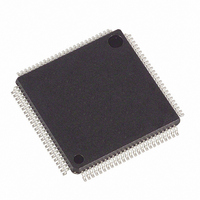
DS21352L+ Maxim Integrated Products, DS21352L+ Datasheet - Page 8

DS21352L+
Manufacturer Part Number
DS21352L+
Description
IC TXRX T1 1-CHIP 3.3V 100-LQFP
Manufacturer
Maxim Integrated Products
Datasheet
1.DS21352L.pdf
(137 pages)
Specifications of DS21352L+
Function
Single-Chip Transceiver
Interface
HDLC, T1
Number Of Circuits
1
Voltage - Supply
3.14 V ~ 3.47 V
Current - Supply
75mA
Operating Temperature
0°C ~ 70°C
Mounting Type
Surface Mount
Package / Case
100-LQFP
Includes
DSX-1 and CSU Line Build-Out Generator, HDLC Controller, In-Band Loop Code Generator and Detector
Lead Free Status / RoHS Status
Lead free / RoHS Compliant
Power (watts)
-
3.1 FUNCTIONAL DESCRIPTION
The analog AMI/B8ZS waveform off of the T1 line is transformer coupled into the RRING and RTIP
pins of the DS21352/552. The device recovers clock and data from the analog signal and passes it
through the jitter attenuation mux to the receive side framer where the digital serial stream is analyzed to
locate the framing/multi-frame pattern. The DS21352/552 contains an active filter that reconstructs the
analog received signal for the nonlinear losses that occur in transmission. The device has a usable receive
sensitivity of 0 dB to –36 dB, which allows the device to operate on cables up to 6000 feet in length. The
receive side framer locates D4 (SLC–96) or ESF multiframe boundaries as well as detects incoming
alarms including, carrier loss, loss of synchronization, blue (AIS) and yellow alarms. If needed, the
receive side elastic store can be enabled in order to absorb the phase and frequency differences between
the recovered T1 data stream and an asynchronous backplane clock which is provided at the RSYSCLK
input. The clock applied at the RSYSCLK input can be either a 2.048 MHz clock or a 1.544 MHz clock.
The RSYSCLK can be a bursty clock with speeds up to 8.192 MHz.
The transmit side of the DS21352/552 is totally independent from the receive side in both the clock
requirements and characteristics. Data off of a backplane can be passed through a transmit side elastic
store if necessary. The transmit formatter will provide the necessary frame/multiframe data overhead for
T1 transmission. Once the data stream has been prepared for transmission, it is sent via the jitter
attenuation mux to the waveshaping and line driver functions. The DS21352/552 will drive the T1 line
from the TTIP and TRING pins via a coupling transformer. The line driver can handle both long haul
(CSU) and short haul (DSX–1) lines.
Reader’s Note: This data sheet assumes a particular nomenclature of the T1 operating environment. In
each 125 ms frame, there are 24 eight–bit channels plus a framing bit. It is assumed that the framing bit is
sent first followed by channel 1. Each channel is made up of eight bits, which are numbered, 1 to 8. Bit
number 1 is the MSB and is transmitted first. Bit number 8 is the LSB and is transmitted last. The term
“locked” is used to refer to two clock signals that are phase or frequency locked or derived from a
common clock (i.e., a 1.544 MHz clock may be locked to a 2.048MHz clock if they share the same 8 kHz
component). Throughout this data sheet, the following abbreviations will be used:
B8ZS
BOC
CRC
D4
ESF
FDL
FPS
Fs
Ft
HDLC
MF
SLC–96
Bipolar with 8 Zero Substitution
Bit Oriented Code
Cyclical Redundancy Check
Superframe (12 frames per multiframe) Multiframe Structure
Extended Superframe (24 frames per multiframe) Multiframe Structure
Facility Data Link
Framing Pattern Sequence in ESF
Signaling Framing Pattern in D4
Terminal Framing Pattern in D4
High Level Data Link Control
Multiframe
Subscriber Loop Carrier – 96 Channels (SLC–96 is an AT&T registered trademark)
8 of 137


