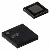
SC16C652BIBS,157 NXP Semiconductors, SC16C652BIBS,157 Datasheet - Page 12

SC16C652BIBS,157
Manufacturer Part Number
SC16C652BIBS,157
Description
IC UART DUAL W/FIFO 32HVQFN
Manufacturer
NXP Semiconductors
Datasheet
1.SC16C652BIB48128.pdf
(43 pages)
Specifications of SC16C652BIBS,157
Features
2 Channels
Number Of Channels
2, DUART
Fifo's
32 Byte
Voltage - Supply
2.5V, 3.3V, 5V
With Auto Flow Control
Yes
With Irda Encoder/decoder
Yes
With False Start Bit Detection
Yes
With Modem Control
Yes
With Cmos
Yes
Mounting Type
Surface Mount
Package / Case
32-VFQFN Exposed Pad
Transmitter And Receiver Fifo Counter
Yes
Data Rate
5Mbps
Operating Supply Voltage (max)
5.5V
Mounting
Surface Mount
Pin Count
32
Operating Temperature (min)
-40C
Operating Temperature (max)
85C
Operating Temperature Classification
Industrial
Lead Free Status / RoHS Status
Lead free / RoHS Compliant
Other names
568-2046
935276387157
SC16C652BIBS
935276387157
SC16C652BIBS
Philips Semiconductors
SC16C652B_4
Product data sheet
6.10 Loop-back mode
6.9 DMA operation
Table 6:
The SC16C652B FIFO trigger level provides additional flexibility to the user for block
mode operation. The user can optionally operate the transmit and receive FIFOs in the
DMA mode (FCR[3]). The DMA mode affects the state of the RXRDY and TXRDY output
pins.
Table 7:
Table 8:
The internal loop-back capability allows on-board diagnostics. In the loop-back mode, the
normal modem interface pins are disconnected and reconfigured for loop-back internally
(see
In the loop-back mode, the transmitter output (TX) and the receiver input (RX) are
disconnected from their associated interface pins, and instead are connected together
internally. The CTS, DSR, CD, and RI are disconnected from their normal modem control
inputs pins, and instead are connected internally to RTS, DTR, MCR[3] (OP2) and
Output
baud rate
(bit/s)
50
75
110
150
300
600
1200
2400
3600
4800
7200
9600
19.2 k
38.4 k
57.6 k
115.2 k
Non-DMA mode
1 = FIFO empty
0 = at least 1 byte in FIFO
Non-DMA mode
1 = at least 1 byte in FIFO
0 = FIFO empty
Figure
Table 7
Baud rate generator programming table using a 1.8432 MHz clock
Effect of DMA mode on state of RXRDY pin
Effect of DMA mode on state of TXRDY pin
5). MCR[3:0] register bits are used for controlling loop-back diagnostic testing.
and
Output
16 clock divisor
(decimal)
2304
1536
1047
768
384
192
96
48
32
24
16
12
6
3
2
1
Table 8
Rev. 04 — 1 September 2005
show this.
DMA mode
0-to-1 transition when FIFO empties
1-to-0 transition when FIFO reaches trigger level, or time-out occurs
DMA mode
0-to-1 transition when FIFO becomes full
1-to-0 transition when FIFO goes below trigger level
Dual UART with 32-byte FIFOs and IrDA encoder/decoder
Output
16 clock divisor
(HEX)
900
600
417
300
180
C0
60
30
20
18
10
0C
06
03
02
01
DLM
program value
(HEX)
09
06
04
03
01
00
00
00
00
00
00
00
00
00
00
00
© Koninklijke Philips Electronics N.V. 2005. All rights reserved.
SC16C652B
DLL
program value
(HEX)
00
00
17
00
80
C0
60
30
20
18
10
0C
06
03
02
01
12 of 43


