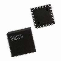
SC16C2552BIA44,512 NXP Semiconductors, SC16C2552BIA44,512 Datasheet - Page 10

SC16C2552BIA44,512
Manufacturer Part Number
SC16C2552BIA44,512
Description
IC UART DUAL SOT187-2
Manufacturer
NXP Semiconductors
Datasheet
1.SC16C2552BIA44529.pdf
(38 pages)
Specifications of SC16C2552BIA44,512
Features
2 Channels
Number Of Channels
2, DUART
Fifo's
16 Byte
Voltage - Supply
2.5V, 3.3V, 5V
With Irda Encoder/decoder
Yes
With False Start Bit Detection
Yes
With Modem Control
Yes
With Cmos
Yes
Mounting Type
Surface Mount
Package / Case
44-LCC (J-Lead)
Lead Free Status / RoHS Status
Lead free / RoHS Compliant
Other names
935274408512
SC16C2552BIA44
SC16C2552BIA44
SC16C2552BIA44
SC16C2552BIA44
NXP Semiconductors
SC16C2552B_3
Product data sheet
Fig 4.
RXRDYA, RXRDYB
TXRDYA, TXRDYB
INTA, INTB
D0 to D7
A0 to A2
Internal Loopback mode diagram
RESET
CHSEL
IOW
IOR
CS
SC16C2552B
made available at the user data interface D0 to D7. The user optionally compares the
received data to the initial transmitted data for verifying error-free operation of the UART
TX/RX circuits.
In this mode, the receiver and transmitter interrupts are fully operational. The Modem
Control Interrupts are also operational. However, the interrupts can only be read using
lower four bits of the Modem Status Register (MSR[3:0]) instead of the four Modem Status
Register bits 7:4. The interrupts are still controlled by the IER.
INTERRUPT
REGISTER
CONTROL
CONTROL
DATA BUS
SELECT
LOGIC
LOGIC
LOGIC
AND
5 V, 3.3 V and 2.5 V dual UART, 5 Mbit/s (max.), with 16-byte FIFOs
Rev. 03 — 12 February 2009
XTAL1
REGISTERS
REGISTERS
GENERATOR
CLOCK AND
BAUD RATE
TRANSMIT
RECEIVE
FIFO
FIFO
XTAL2
TRANSMIT
REGISTER
REGISTER
RECEIVE
CONTROL
SHIFT
SHIFT
MODEM
LOGIC
SC16C2552B
MCR[4] = 1
002aaa489
© NXP B.V. 2009. All rights reserved.
TXA, TXB
RXA, RXB
RTSA, RTSB
CTSA, CTSB
DTRA, DTRB
DSRA, DSRB
(OP1A, OP1B)
RIA, RIB
(OP2A, OP2B)
CDA, CDB
10 of 38


