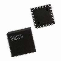
SC16C2552BIA44,512 NXP Semiconductors, SC16C2552BIA44,512 Datasheet - Page 9

SC16C2552BIA44,512
Manufacturer Part Number
SC16C2552BIA44,512
Description
IC UART DUAL SOT187-2
Manufacturer
NXP Semiconductors
Datasheet
1.SC16C2552BIA44529.pdf
(38 pages)
Specifications of SC16C2552BIA44,512
Features
2 Channels
Number Of Channels
2, DUART
Fifo's
16 Byte
Voltage - Supply
2.5V, 3.3V, 5V
With Irda Encoder/decoder
Yes
With False Start Bit Detection
Yes
With Modem Control
Yes
With Cmos
Yes
Mounting Type
Surface Mount
Package / Case
44-LCC (J-Lead)
Lead Free Status / RoHS Status
Lead free / RoHS Compliant
Other names
935274408512
SC16C2552BIA44
SC16C2552BIA44
SC16C2552BIA44
SC16C2552BIA44
NXP Semiconductors
SC16C2552B_3
Product data sheet
6.6 DMA operation
6.7 Loopback mode
Table 5.
The SC16C2552B FIFO trigger level provides additional flexibility to the user for block
mode operation. LSR[6:5] provide an indication when the transmitter is empty or has an
empty location(s). The user can optionally operate the transmit and receive FIFOs in the
DMA mode (FCR[3]). When the transmit and receive FIFOs are enabled and the DMA
mode is de-activated (DMA Mode 0), the SC16C2552B activates the interrupt output pin
for each data transmit or receive operation. When DMA mode is activated (DMA Mode 1),
the user takes the advantage of block mode operation by loading or unloading the FIFO in
a block sequence determined by the receive trigger level and the transmit FIFO. In this
mode, the SC16C2552B sets the interrupt output pin when characters in the transmit
FIFO is below 16, or the characters in the receive FIFOs are above the receive trigger
level.
The internal loopback capability allows on-board diagnostics. In the Loopback mode, the
normal modem interface pins are disconnected and reconfigured for loopback internally.
MCR[3:0] register bits are used for controlling loopback diagnostic testing. In the
Loopback mode, INT enable and MCR[2] in the MCR register (bits 3:2) control the modem
RI and CD inputs, respectively. MCR signals DTR (bit 0) and RTS (bit 1) are used to
control the modem DSR and CTS inputs, respectively. The transmitter output (TX) and the
receiver input (RX) are disconnected from their associated interface pins, and instead are
connected together internally (see
disconnected from their normal modem control inputs pins, and instead are connected
internally to RTS, DTR, OP2 and OP1. Loopback test data is entered into the transmit
holding register via the user data bus interface, D0 to D7. The transmit UART serializes
the data and passes the serial data to the receive UART via the internal loopback
connection. The receive UART converts the serial data back into parallel data that is then
Output
baud rate
50
75
150
300
600
1200
2400
4800
7200
9600
19.2 k
38.4 k
57.6 k
115.2 k
Baud rate generator programming table using a 1.8432 MHz clock
Output
16 clock divisor
(decimal)
2304
1536
768
384
192
96
48
24
16
12
6
3
2
1
5 V, 3.3 V and 2.5 V dual UART, 5 Mbit/s (max.), with 16-byte FIFOs
Rev. 03 — 12 February 2009
Figure
Output
16 clock divisor
(HEX)
900
600
300
180
C0
60
30
18
10
0C
06
03
02
01
4). The CTS, DSR, CD, and RI are
DLM
program value
(HEX)
09
06
03
01
00
00
00
00
00
00
00
00
00
00
SC16C2552B
© NXP B.V. 2009. All rights reserved.
DLL
program value
(HEX)
00
00
00
80
C0
60
30
18
10
0C
06
03
02
01
9 of 38


