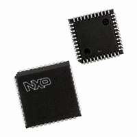
SC16C2552BIA44,512 NXP Semiconductors, SC16C2552BIA44,512 Datasheet - Page 6

SC16C2552BIA44,512
Manufacturer Part Number
SC16C2552BIA44,512
Description
IC UART DUAL SOT187-2
Manufacturer
NXP Semiconductors
Datasheet
1.SC16C2552BIA44529.pdf
(38 pages)
Specifications of SC16C2552BIA44,512
Features
2 Channels
Number Of Channels
2, DUART
Fifo's
16 Byte
Voltage - Supply
2.5V, 3.3V, 5V
With Irda Encoder/decoder
Yes
With False Start Bit Detection
Yes
With Modem Control
Yes
With Cmos
Yes
Mounting Type
Surface Mount
Package / Case
44-LCC (J-Lead)
Lead Free Status / RoHS Status
Lead free / RoHS Compliant
Other names
935274408512
SC16C2552BIA44
SC16C2552BIA44
SC16C2552BIA44
SC16C2552BIA44
NXP Semiconductors
6. Functional description
SC16C2552B_3
Product data sheet
6.1 UART A-B functions
The SC16C2552B provides serial asynchronous receive data synchronization,
parallel-to-serial and serial-to-parallel data conversions for both the transmitter and
receiver sections. These functions are necessary for converting the serial data stream into
parallel data that is required with digital data systems. Synchronization for the serial data
stream is accomplished by adding start and stop bits to the transmit data to form a data
character. Data integrity is ensured by attaching a parity bit to the data character. The
parity bit is checked by the receiver for any transmission bit errors. The SC16C2552B is
fabricated with an advanced CMOS process.
The SC16C2552B is an upward solution that provides a dual UART capability with
16 bytes of transmit and receive FIFO memory, instead of none in the 16C450. The
SC16C2552B is designed to work with high speed modems and shared network
environments that require fast data processing time. Increased performance is realized in
the SC16C2552B by the transmit and receive FIFOs. This allows the external processor to
handle more networking tasks within a given time. In addition, the four selectable receive
FIFO trigger interrupt levels are uniquely provided for maximum data throughput
performance, especially when operating in a multi-channel environment. The FIFO
memory greatly reduces the bandwidth requirement of the external controlling CPU,
increases performance, and reduces power consumption.
The SC16C2552B is capable of operation up to 1.5 Mbit/s with a 24 MHz crystal. With a
crystal or external clock input of 7.3728 MHz, the user can select data rates up to
460.8 kbit/s.
The rich feature set of the SC16C2552B is available through internal registers. Selectable
receive FIFO trigger levels, selectable TX and RX baud rates, and modem interface
controls are all standard features.
The UART provides the user with the capability to bidirectionally transfer information
between an external CPU, the SC16C2552B package, and an external serial device. A
logic 0 on chip select pin CS and a logic 1 on CHSEL allows the user to configure, send
data, and/or receive data via UART channel A. A logic 0 on chip select pin CS and a
logic 0 on CHSEL allows the user to configure, send data, and/or receive data via UART
channel B. Individual channel select functions are shown in
Table 3.
During a write mode cycle, the setting of AFR[0] to a logic 1 will override the CHSEL
selection and allow a simultaneous write to both UART channel sections. This functional
capability allows the registers in both UART channels to be modified concurrently, saving
individual channel initialization time. Caution should be considered, however, when using
this capability. Any in-process serial data transfer may be disrupted by changing an active
channel’s mode.
Chip select
CS = 1
CS = 0
Serial port selection
UART select
none
UART channel selected as follows:
CHSEL = 1: UART channel A
CHSEL = 0: UART channel B
5 V, 3.3 V and 2.5 V dual UART, 5 Mbit/s (max.), with 16-byte FIFOs
Rev. 03 — 12 February 2009
Table
SC16C2552B
3.
© NXP B.V. 2009. All rights reserved.
6 of 38


