IS82C50A-5Z Intersil, IS82C50A-5Z Datasheet - Page 4
IS82C50A-5Z
Manufacturer Part Number
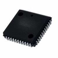
IS82C50A-5Z
Description
IC PERIPH UART/BRG 10MHZ 44-PLCC
Manufacturer
Intersil
Datasheet
1.CS82C50A-5Z.pdf
(25 pages)
Specifications of IS82C50A-5Z
Features
Single Chip UART/BRG
Number Of Channels
1, UART
Protocol
RS232C
Voltage - Supply
4.5 V ~ 5.5 V
With Parallel Port
Yes
With False Start Bit Detection
Yes
With Modem Control
Yes
With Cmos
Yes
Mounting Type
Surface Mount
Package / Case
44-LCC (J-Lead)
Lead Free Status / RoHS Status
Lead free / RoHS Compliant
Available stocks
Company
Part Number
Manufacturer
Quantity
Price


Pin Description
DISTR,
DISTR
DOSTR,
DOSTR
D0-D7
A0, A1,
A2
XTAL1,
XTAL2
SOUT
GND
CTS
DSR
DTR
RTS
BAUDOUT
SYMBOL
NUMBER
28, 27,
PIN
1-8
22
21
19
18
26
16
17
11
20
36
37
33
32
15
TYPE
4
I/O
O
O
O
O
O
I
I
I
I
I
I
I
I
I
ACTIVE
LEVEL
H
H
H
L
L
L
L
L
L
L
DATA IN STROBE, DATA IN STROBE: DISTR, DISTR are read inputs which cause the
82C50A to output data to the data bus (D0-D7). The data output depends upon the
register selected by the address inputs A0, A1, A2. The chip select inputs CS0, CS1,
CS2 enable the DISTR, DISTR inputs.
Only an active DISTR or DISTR, not both, is used to receive data from the 82C50A
during a read operation. If DISTR is used as the read input, DlSTR should be tied high.
If DISTR is used as the active read input, DISTR should be tied low.
DATA OUT STROBE, DATA OUT STROBE: DOSTR, DOSTR are write inputs which
cause data from the data bus (D0-D7) to be input to the 82C50A. The data input depends
upon the register selected by the address inputs A0, A1, A2. The chip select inputs CS0,
CS1, CS2 enable the DOSTR, DOSTR inputs.
Only an active DOSTR or DOSTR, not both, is used to transmit data to the 82C50A
during a write operation. If DOSTR is used as the write input, DOSTR should be tied
high. If DOSTR is used as the write input, DOSTR should be tied low.
DATA BITS 0-7: The Data Bus provides eight, three-state input/output lines for the
transfer of data, control and status information between the 82C50A and the CPU. For
character formats of less than 8 bits, D7, D6 and D5 are “don’t cares” for data write
operations and 0 for data read operations. These lines are normally in a high impedance
state except during read operations. D0 is the Least Significant Bit (LSB) and is the first
serial data bit to be received or transmitted.
REGISTER SELECT: The address lines select the internal registers during CPU bus
operations. See Table 1.
CRYSTAL/CLOCK: Crystal connections for the internal Baud Rate Generator. XTAL1
can also be used as an external clock input, in which case XTAL2 should be left open.
SERIAL DATA OUTPUT: Serial data output from the 82C50A transmitter circuitry. A
Mark (1) is a logic one (high) and Space (0) is a logic zero (low). SOUT is held in the
Mark condition when the transmitter is disabled, MR is true, the Transmitter Register is
empty, or when in the Loop Mode. SOUT is not affected by the CTS input.
GROUND: Power supply ground connection (V
CLEAR TO SEND: The logical state of the CTS pin is reflected in the CTS bit of the
(MSR) Modem Status Register (CTS is bit 4 of the MSR, written MSR (4)). A change of
state in the CTS pin since the previous reading of the MSR causes the setting of DCTS
(MSR(O)) of the Modem Status Register. When CTS pin is ACTIVE (low), the modem is
indicating that data on SOUT can be transmitted on the communications link. If CTS pin
goes INACTIVE (high), the 82C50A should not be allowed to transmit data out of SOUT.
CTS pin does not affect Loop Mode operation.
DATA SET READY: The logical state of the DSR pin is reflected in MSR(5) of the
Modem Status Register. DDSR (MSR(1)) indicates whether the DSR pin has changed
state since the previous reading of the MSR. When the DSR pin is ACTIVE (low), the
modem is indicating that it is ready to exchange data with the 82C50A, while the DSR
Pin INACTIVE (high) indicates that the modem is not ready for data exchange. The
ACTIVE condition indicates only the condition of the local Data Communications
Equipment (DCE), and does not imply that a data circuit as been established with remote
equipment.
DATA TERMINAL READY: The DTR pin can be set (low) by writing a logic 1 to MCR(0),
Modem Control Register bit 0. This signal is cleared (high) by writing a logic 0 to the DTR
bit (MCR(0)) or whenever a MR ACTIVE (high) is applied to the 82C50A. When ACTIVE
(low), DTR pin indicates to the DCE that the 82C50A is ready to receive data. In some
instances, DTR pin is used as a power on indicator. The INACTIVE (high) state causes
the DCE to disconnect the modem from the telecommunications circuit.
REQUEST TO SEND: The RTS signal is an output used to enable the modem. The RTS
pin is set low by writing a logic 1 to MCR (1) bit 1 of the Modem Control Register. The
RTS pin is reset high by Master Reset. When ACTIVE, the RTS pin indicates to the DCE
that the 82C50A has data ready to transmit. In half duplex operations, RTS is used to
control the direction of the line.
BAUDOUT: This output is a 16X clock out used for the transmitter section (16X = 16
times the data rate). The BAUDOUT clock rate is equal to the reference oscillator
frequency divided by the specified divisor in the Baud Rate Generator Divisor Latches
DLL and DLM. BAUDOUT may be used by the Receiver section by tying this output to
RCLK.
82C50A
DESCRIPTION
SS
).
August 24, 2006
FN2958.5
Related parts for IS82C50A-5Z
Image
Part Number
Description
Manufacturer
Datasheet
Request
R

Part Number:
Description:
Intersil Corporation [CMOS Serial Controller Interface]
Manufacturer:
Intersil Corporation
Datasheet:
Part Number:
Description:
Manufacturer:
Intersil Corporation
Datasheet:
Part Number:
Description:
357-036-542-201 CARDEDGE 36POS DL .156 BLK LOPRO
Manufacturer:
Intersil Corporation
Datasheet:
Part Number:
Description:
1024-Word x 4-Bit LSI Static RAM
Manufacturer:
Intersil Corporation
Datasheet:
Part Number:
Description:
General Purpose NPN Transistor Arrays FN341.4
Manufacturer:
Intersil Corporation
Datasheet:
Part Number:
Description:
CMOS 16-Bit Microprocessor
Manufacturer:
Intersil Corporation
Datasheet:
Part Number:
Description:
Manufacturer:
Intersil Corporation
Datasheet:
Part Number:
Description:
Manufacturer:
Intersil Corporation
Datasheet:
Part Number:
Description:
Manufacturer:
Intersil Corporation
Datasheet:
Part Number:
Description:
Manufacturer:
Intersil Corporation
Datasheet:
Part Number:
Description:
CMOS 6-Bit Latch and Decoder Memory Interfaces
Manufacturer:
Intersil Corporation
Datasheet:
Part Number:
Description:
CA3046General Purpose NPN Transistor Arrays
Manufacturer:
Intersil Corporation
Datasheet:
Part Number:
Description:
Manufacturer:
Intersil Corporation
Datasheet:
Part Number:
Description:
TR909 DLC/FLC SLIC with Low Power Standby
Manufacturer:
Intersil Corporation
Datasheet:
Part Number:
Description:
Manufacturer:
Intersil Corporation
Datasheet: