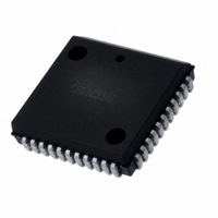
IS82C50A-5Z Intersil, IS82C50A-5Z Datasheet - Page 7

IS82C50A-5Z
Manufacturer Part Number
IS82C50A-5Z
Description
IC PERIPH UART/BRG 10MHZ 44-PLCC
Manufacturer
Intersil
Datasheet
1.CS82C50A-5Z.pdf
(25 pages)
Specifications of IS82C50A-5Z
Features
Single Chip UART/BRG
Number Of Channels
1, UART
Protocol
RS232C
Voltage - Supply
4.5 V ~ 5.5 V
With Parallel Port
Yes
With False Start Bit Detection
Yes
With Modem Control
Yes
With Cmos
Yes
Mounting Type
Surface Mount
Package / Case
44-LCC (J-Lead)
Lead Free Status / RoHS Status
Lead free / RoHS Compliant
Available stocks
Company
Part Number
Manufacturer
Quantity
Price
Accessible Registers
The three types of internal registers in the 82C50A used in
the operation of the device are control, status, and data
registers. The control registers are the Bit Rate Select
Register DLL and DLM, Line Control Register, Interrupt
Enable Register and the Modem Control registers, while the
status registers are the Line Status Registers and the
Modem Status Register. The data registers are the Receiver
Buffer Register and Transmitter Holding Register. The
Address, Read, and Write inputs are used in conjunction
with the Divisor Latch Access Bit in the Line Control Register
(LCR(7)) to select the register to be written or read (see
Table 1.). Individual bits within these registers are referred to
by the register mnemonic and the bit number in parenthesis.
An example, LCR(7) refers to Line Control Register Bit 7.
The Transmitter Buffer Register and Receiver Buffer
Register are data registers holding from 5-8 data bits. If less
than eight data bits are transmitted, data is right justified to
the LSB. Bit 0 of a data word is always the first serial data bit
received and transmitted. The 82C50A data registers are
double buffered so that read and write operations can be
performed at the same time the UART is performing the
parallel to serial and serial to parallel conversion. This
provides the microprocessor with increased flexibility in its
read and write timing.
Line Control Register (LCR)
LCR
7
LCR
6
LCR
5
LCR
4
LCR
3
7
LCR
2
LCR
1
LCR
0
Word
Length
Select
Stop
Bit
Select
Parity
Enable
Even Parity
Select
Stick Parity
Break
Control
Divisor Latch
Access Bit
82C50A
0 0 = 5 Data Bits
0 1 = 6 Data Bits
1 0 = 7 Data Bits
1 1 = 8 Data Bits
0 = 1 Stop Bit
1 = 1.5 Stop Bits if 5 Data Bit Word Length is Selected 2 Stop Bits if 6,
0 = Parity Disabled
1 = Parity Enabled (Generated & Checked)
0 = Odd Parity When Parity is Enabled
1 = Even Parity When Parity is Enabled
0 = Stick Parity Disabled
1 = When Parity is Enabled Forces the Transmission and Checking of
0 = Break Disabled
1 = Break Enabled. The Serial Output (SOUT) is Forced to the Spacing
0 = Must be Low to Access the Receiver Buffer. Transmitter Holding
1 = Must be High to Access the Divisor Latches DLL and DLM of the
NOTE: X = “Don’t Care”, 0 = Logic Low, 1 = Logic High
7, or 8 Data Bit Word Length is Selected
a Parity Bit of a Known State. Parity Bit Forced to a Logic 1 if LCR
(4) = 0 or to a Logic 0 If LCR (4) = 1.
(Logic 0) State.
Register or the Interrupt Enable Register.
Baud Rate Generator During a Read or Write Operation.
DLAB
X
X
X
X
X
X
0
0
0
1
1
TABLE 1. ACCESSING 82C50A INTERNAL REGISTERS
A2
0
0
0
0
0
1
1
1
1
0
0
A1
0
0
0
1
1
0
0
1
1
0
0
A0
0
0
1
0
1
0
1
0
1
0
1
MNEMONIC
MCR
MSR
RBR
THR
LCR
SCR
DLM
LSR
DLL
lER
IIR
Receiver Buffer
Register (read only)
Transmitter Holding
Register (write only)
Interrupt Enable
Register
Interrupt Identification
Register
(read only)
Line Control Register
Modem Control
Register
Line Status Register
Modem Status
Register
Scratch Register
Divisor Latch (LSB)
Divisor Latch (MSB)
REGISTER
August 24, 2006
FN2958.5


