SC16C654IA68,529 NXP Semiconductors, SC16C654IA68,529 Datasheet - Page 10
SC16C654IA68,529
Manufacturer Part Number
SC16C654IA68,529
Description
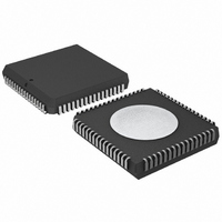
IC UART QUAD W/FIFO 68-PLCC
Manufacturer
NXP Semiconductors
Datasheet
1.SC16C654DIB64151.pdf
(52 pages)
Specifications of SC16C654IA68,529
Number Of Channels
4, QUART
Fifo's
64 Byte
Voltage - Supply
2.5V, 3.3V, 5V
With Auto Flow Control
Yes
With Irda Encoder/decoder
Yes
With False Start Bit Detection
Yes
With Modem Control
Yes
With Cmos
Yes
Mounting Type
Surface Mount
Package / Case
68-LCC (J-Lead)
Lead Free Status / RoHS Status
Lead free / RoHS Compliant
Other names
568-3282-5
935270051529
SC16C654IA68-S
935270051529
SC16C654IA68-S
Available stocks
Company
Part Number
Manufacturer
Quantity
Price
Company:

Part Number:
SC16C654IA68,529
Manufacturer:
NXP Semiconductors
Quantity:
10 000


Philips Semiconductors
Table 2:
9397 750 11617
Product data
Symbol
RTSA, RTSB,
RTSC, RTSD
R/W
RXA, RXB,
RXC, RXD
RXRDY
TXA, TXB,
TXC, TXD
TXRDY
V
XTAL1
XTAL2
CC
Pin description
Pin
PLCC68 LQFP64
14, 22,
48, 56
18
7, 29,
41, 63
38
17, 19,
51, 53
39
13, 47,
64
35
36
5, 13,
36, 44
-
62, 20,
29, 51
-
8, 10,
39, 41
-
4, 21,
35, 52
25
26
…continued
Type
O
I
I
O
O
O
I
I
O
Description
Request to Send (Active-LOW). These outputs are associated with individual
UART channels, A through D. A logic 0 on the RTS pin indicates the transmitter
has data ready and waiting to send. Writing a logic 1 in the modem control
register MCR[1] will set this pin to a logic 0, indicating data is available. After a
reset this pin will be set to a logic 1. This pin only affects the transmit and
receive operations when Auto RTS function is enabled via the Enhanced
Feature Register (EFR[6]) for hardware flow control operation.
Read/Write strobe. This function is associated with the 68 mode only. This pin
provides the combined functions for Read or Write strobes.
Logic 1 = Read from UART register selected by CS and A0-A4.
Logic 0 = Write to UART register selected by CS and A0-A4.
Receive data input RXA-RXD. These inputs are associated with individual
serial channel data to the SC16C654/654D. The RX signal will be a logic 1
during reset, idle (no data), or when the transmitter is disabled. During the local
loop-back mode, the RX input pin is disabled and TX data is connected to the
UART RX input internally.
Receive Ready (Active-LOW). This function is associated with 68-pin package
only. RXRDY contains the wire-ORed status of all four receive channel FIFOs,
RXRDYA-RXRDYD. A logic 0 indicates receive data ready status, i.e., the RHR
is full, or the FIFO has one or more RX characters available for unloading. This
pin goes to a logic 1 when the FIFO/RHR is empty, or when there are no more
characters available in either the FIFO or RHR. Individual channel RX status is
read by examining individual internal registers via CS and A0-A4 pin functions.
Transmit data A, B, C, D. These outputs are associated with individual serial
transmit channel data from the SC16C654/654D. The TX signal will be a logic 1
during reset, idle (no data), or when the transmitter is disabled. During the local
loop-back mode, the TX output pin is disabled and TX data is internally
connected to the UART RX input.
Transmit Ready (Active-LOW). This function is associated with the 68-pin
package only. TXRDY contains the wire-ORed status of all four transmit
channel FIFOs, TXRDYA-TXRDYD. A logic 0 indicates a buffer ready status,
i.e., at least one location is empty and available in one of the TX channels
(A-D). This pin goes to a logic 1 when all four channels have no more empty
locations in the TX FIFO or THR. Individual channel TX status can be read by
examining individual internal registers via CS and A0-A4 pin functions.
Power supply inputs.
Crystal or external clock input. Functions as a crystal input or as an external
clock input. A crystal can be connected between this pin and XTAL2 to form an
internal oscillator circuit (see
connected to this pin to provide custom data rates. (See
“Programmable baud rate
Output of the crystal oscillator or buffered clock. (See also XTAL1.) Crystal
oscillator output or buffered clock output.
Quad UART with 64-byte FIFO and infrared (IrDA) encoder/decoder
Rev. 04 — 19 June 2003
generator”.)
Figure
6). Alternatively, an external clock can be
SC16C654/654D
© Koninklijke Philips Electronics N.V. 2003. All rights reserved.
Section 6.11
10 of 52
Related parts for SC16C654IA68,529
Image
Part Number
Description
Manufacturer
Datasheet
Request
R

Part Number:
Description:
NXP Semiconductors designed the LPC2420/2460 microcontroller around a 16-bit/32-bitARM7TDMI-S CPU core with real-time debug interfaces that include both JTAG andembedded trace
Manufacturer:
NXP Semiconductors
Datasheet:

Part Number:
Description:
NXP Semiconductors designed the LPC2458 microcontroller around a 16-bit/32-bitARM7TDMI-S CPU core with real-time debug interfaces that include both JTAG andembedded trace
Manufacturer:
NXP Semiconductors
Datasheet:
Part Number:
Description:
NXP Semiconductors designed the LPC2468 microcontroller around a 16-bit/32-bitARM7TDMI-S CPU core with real-time debug interfaces that include both JTAG andembedded trace
Manufacturer:
NXP Semiconductors
Datasheet:
Part Number:
Description:
NXP Semiconductors designed the LPC2470 microcontroller, powered by theARM7TDMI-S core, to be a highly integrated microcontroller for a wide range ofapplications that require advanced communications and high quality graphic displays
Manufacturer:
NXP Semiconductors
Datasheet:
Part Number:
Description:
NXP Semiconductors designed the LPC2478 microcontroller, powered by theARM7TDMI-S core, to be a highly integrated microcontroller for a wide range ofapplications that require advanced communications and high quality graphic displays
Manufacturer:
NXP Semiconductors
Datasheet:
Part Number:
Description:
The Philips Semiconductors XA (eXtended Architecture) family of 16-bit single-chip microcontrollers is powerful enough to easily handle the requirements of high performance embedded applications, yet inexpensive enough to compete in the market for hi
Manufacturer:
NXP Semiconductors
Datasheet:
Part Number:
Description:
The XA-S3 device is a member of Philips Semiconductors? XA(eXtended Architecture) family of high performance 16-bitsingle-chip microcontrollers
Manufacturer:
NXP Semiconductors
Datasheet:

Part Number:
Description:
The NXP BlueStreak LH75401/LH75411 family consists of two low-cost 16/32-bit System-on-Chip (SoC) devices
Manufacturer:
NXP Semiconductors
Datasheet:
Part Number:
Description:
The NXP LPC3130/3131 combine an 180 MHz ARM926EJ-S CPU core, high-speed USB2
Manufacturer:
NXP Semiconductors
Datasheet:
Part Number:
Description:
The NXP LPC3141 combine a 270 MHz ARM926EJ-S CPU core, High-speed USB 2
Manufacturer:
NXP Semiconductors
Part Number:
Description:
The NXP LPC3143 combine a 270 MHz ARM926EJ-S CPU core, High-speed USB 2
Manufacturer:
NXP Semiconductors

Part Number:
Description:
The NXP LPC3152 combines an 180 MHz ARM926EJ-S CPU core, High-speed USB 2
Manufacturer:
NXP Semiconductors
Part Number:
Description:
The NXP LPC3154 combines an 180 MHz ARM926EJ-S CPU core, High-speed USB 2
Manufacturer:
NXP Semiconductors

Part Number:
Description:
Standard level N-channel enhancement mode Field-Effect Transistor (FET) in a plastic package using NXP High-Performance Automotive (HPA) TrenchMOS technology
Manufacturer:
NXP Semiconductors
Datasheet: