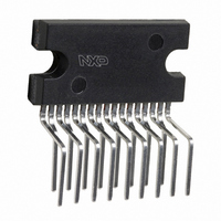
TDA8947J/N3,112 NXP Semiconductors, TDA8947J/N3,112 Datasheet - Page 9

TDA8947J/N3,112
Manufacturer Part Number
TDA8947J/N3,112
Description
IC AMP AUDIO PWR 29W QUAD 17SIL
Manufacturer
NXP Semiconductors
Type
Class ABr
Datasheet
1.TDA8947JN3112.pdf
(24 pages)
Specifications of TDA8947J/N3,112
Output Type
4-Channel (Quad)
Package / Case
17-SIL (Bent and Staggered Leads)
Max Output Power X Channels @ Load
29W x 2 @ 8 Ohm; 14W x 4 @ 4 Ohm
Voltage - Supply
9 V ~ 26 V
Features
Depop, Mute, Short-Circuit and Thermal Protection, Standby
Mounting Type
Through Hole
Product
Class-AB
Output Power
29 W
Available Set Gain
32 dB
Thd Plus Noise
0.05 %
Operating Supply Voltage
18 V
Maximum Power Dissipation
69000 mW
Maximum Operating Temperature
+ 85 C
Mounting Style
Through Hole
Audio Load Resistance
8 Ohms
Input Signal Type
Single
Minimum Operating Temperature
- 40 C
Output Signal Type
Differential, Single
Supply Type
Single
Supply Voltage (max)
26 V
Supply Voltage (min)
9 V
Lead Free Status / RoHS Status
Lead free / RoHS Compliant
Other names
568-3458-5
935274472112
TDA8947J
935274472112
TDA8947J
Philips Semiconductors
11. Static characteristics
Table 8:
V
otherwise specified.
[1]
[2]
[3]
[4]
[5]
[6]
12. Dynamic characteristics
Table 9:
V
otherwise specified.
9397 750 14938
Product data sheet
Symbol
Supply
V
I
I
Output pins
V
Mode selection pins
V
V
I
I
Symbol
P
THD
G
Z
q
stb
MODE1
MODE2
CC
CC
V
i
CC
O
MODE1
MODE2
o(SE)
v
OUT
= 18 V; T
A minimum load is required at supply voltages of V
The amplifier can deliver output power with non clipping output signals into nominal loads as long as the ratings of the IC are not
exceeded.
With a load connected at the outputs the quiescent current will increase.
The DC output voltage, with respect to ground, is approximately 0.5V
Channels 3 and 4 can only be set to Mute or On mode by MODE2 when V
= 18 V; T
V
OUT
= V
Static characteristics
Dynamic characteristics SE
Parameter
SE output power
total harmonic distortion
voltage gain
input impedance
amb
amb
OUT+
Parameter
supply voltage
quiescent supply current
standby supply current
DC output voltage
differential output voltage offset BTL mode
selection voltage on pin
MODE1
selection voltage on pin
MODE2
selection current on pin MODE1 0 V < V
selection current on pin MODE2 0 V < V
= 25 C; R
= 25 C; R
V
OUT-
L
L
= 8 ; V
= 4 ; f = 1 kHz; V
MODE1
= V
Conditions
V
V
P
CC
CC
o
CC
THD = 10 %; R
THD = 0.5 %; R
THD = 10 %; R
MODE1
Conditions
operating
no (clipping) signal
R
On mode
Mute mode
Standby mode
On mode: channels 3 and 4
Mute mode: channels 3 and 4
CC
= 1 W
; V
Rev. 02 — 16 June 2005
= 18 V; see
= 22 V
L
> 22 V: R
=
MODE2
= V
MODE1
MODE2
CC
= V
L
; V
= 3
Figure
CC
< (V
< (V
L
L
MODE2
L
= 4
= 4
CC
; V
= 4
for SE and R
CC
CC
.
i
= 0 V; measured in test circuit
8a
MODE1
= V
3.5 V)
3.5 V)
CC
> V
; measured in test circuit
L
CC
= 6
[1]
[2]
[3]
[4]
[5]
[6]
Min
7
-
-
-
25
40
2.0 V.
Min
9
-
-
-
-
-
V
4.5
0
V
0
-
-
for BTL.
CC
CC
© Koninklijke Philips Electronics N.V. 2005. All rights reserved.
2.0 -
2.0 -
Typ
8.5
6.5
14
0.1
26
60
4-channel audio amplifier
Typ
18
-
100
-
9
-
-
-
-
-
-
Figure
TDA8947J
Figure
Max
-
-
-
0.5
27
-
Max
26
28
145
10
-
170
V
V
0.8
V
V
20
20
12; unless
CC
CC
CC
CC
12; unless
3.5 V
3.5 V
Unit
W
W
W
%
dB
k
Unit
V
V
mA
V
mV
V
V
V
9 of 24
A
A
A


