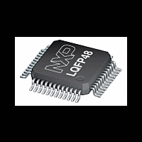
LPC1114FBD48 NXP Semiconductors, LPC1114FBD48 Datasheet - Page 26

LPC1114FBD48
Manufacturer Part Number
LPC1114FBD48
Description
The LPC1114FBD48 is an ARM Cortex-M0 microcontroller and it can operate up to 50 MHz
Manufacturer
NXP Semiconductors
Datasheet
1.LPC1110FD20.pdf
(103 pages)
Available stocks
Company
Part Number
Manufacturer
Quantity
Price
Company:
Part Number:
LPC1114FBD48
Manufacturer:
MARVELL
Quantity:
560
Part Number:
LPC1114FBD48
Manufacturer:
NXP/恩智浦
Quantity:
20 000
Company:
Part Number:
LPC1114FBD48/301
Manufacturer:
NXP
Quantity:
4
Part Number:
LPC1114FBD48/301
Manufacturer:
NXP/恩智浦
Quantity:
20 000
Company:
Part Number:
LPC1114FBD48/301,1
Manufacturer:
SAMSUNG
Quantity:
1 085
Company:
Part Number:
LPC1114FBD48/301,1
Manufacturer:
NXP Semiconductors
Quantity:
10 000
Company:
Part Number:
LPC1114FBD48/3011
Manufacturer:
NXP
Quantity:
5 000
Company:
Part Number:
LPC1114FBD48/301:1
Manufacturer:
NXP Semiconductors
Quantity:
10 000
Part Number:
LPC1114FBD48/302
Manufacturer:
NXP/恩智浦
Quantity:
20 000
Company:
Part Number:
LPC1114FBD48/302,1
Manufacturer:
NXP Semiconductors
Quantity:
10 000
Part Number:
LPC1114FBD48/303
Manufacturer:
NXP/恩智浦
Quantity:
20 000
NXP Semiconductors
Table 9.
[1]
[2]
[3]
[4]
[5]
LPC111X
Product data sheet
Symbol
PIO2_3/RI/MOSI1
PIO2_4
PIO2_5
PIO2_6
PIO2_7
PIO2_8
PIO2_9
PIO2_10
PIO2_11/SCK0
PIO3_0 to PIO3_5
PIO3_0/DTR
PIO3_1/DSR
PIO3_2/DCD
PIO3_3/RI
PIO3_4
PIO3_5
V
XTALIN
XTALOUT
V
DD
SS
Pin state at reset for default function: I = Input; O = Output; PU = internal pull-up enabled (pins pulled up to 2.6 V for
LPC111x/101/201/301, pins pulled up to full V
enabled.
See
reset the chip and wake up from Deep power-down mode. An external pull-up resistor is required on this pin for the Deep power-down
mode.
5 V tolerant pad providing digital I/O functions with configurable pull-up/pull-down resistors and configurable hysteresis (see
I
5 V tolerant pad providing digital I/O functions with configurable pull-up/pull-down resistors, configurable hysteresis, and analog input.
When configured as a ADC input, digital section of the pad is disabled and the pin is not 5 V tolerant (see
2
C-bus pads compliant with the I
Figure 46
LPC1100 and LPC1100L series: LPC1113/14 pin description table (LQFP48 package)
for the reset pad configuration. RESET functionality is not available in Deep power-down mode. Use the WAKEUP pin to
Pin
38
19
20
1
11
12
24
25
31
36
37
43
48
18
21
8; 44
6
7
5; 41
[3]
[6]
[6]
[3]
[3]
[3]
[3]
[3]
[3]
[3]
[3]
[3]
[3]
[3]
[3]
[3]
[3]
Start
logic
input
no
no
no
no
no
no
no
no
no
no
no
no
no
no
no
-
-
-
-
2
C-bus specification for I
Type
I/O
I
I/O
I/O
I/O
I/O
I/O
I/O
I/O
I/O
I/O
I/O
I/O
O
I/O
I
I/O
I
I/O
I
I/O
I/O
I
I
O
I
I/O
All information provided in this document is subject to legal disclaimers.
DD
level on LPC111x/002/102/202/302 (V
Rev. 7 — 1 March 2012
Reset
state
[1]
I; PU
-
-
I; PU
I; PU
I; PU
I; PU
I; PU
I; PU
I; PU
I; PU
-
I; PU
-
I; PU
-
I; PU
-
I; PU
-
I; PU
I; PU
-
-
-
-
2
C standard mode and I
Description
PIO2_3 — General purpose digital input/output pin.
RI — Ring Indicator input for UART.
MOSI1 — Master Out Slave In for SPI1.
PIO2_4 — General purpose digital input/output pin.
PIO2_5 — General purpose digital input/output pin.
PIO2_6 — General purpose digital input/output pin.
PIO2_7 — General purpose digital input/output pin.
PIO2_8 — General purpose digital input/output pin.
PIO2_9 — General purpose digital input/output pin.
PIO2_10 — General purpose digital input/output pin.
PIO2_11 — General purpose digital input/output pin.
SCK0 — Serial clock for SPI0.
Port 3 — Port 3 is a 12-bit I/O port with individual direction and
function controls for each bit. The operation of port 3 pins
depends on the function selected through the IOCONFIG
register block. Pins PIO3_6 to PIO3_11 are not available.
PIO3_0 — General purpose digital input/output pin.
DTR — Data Terminal Ready output for UART.
PIO3_1 — General purpose digital input/output pin.
DSR — Data Set Ready input for UART.
PIO3_2 — General purpose digital input/output pin.
DCD — Data Carrier Detect input for UART.
PIO3_3 — General purpose digital input/output pin.
RI — Ring Indicator input for UART.
PIO3_4 — General purpose digital input/output pin.
PIO3_5 — General purpose digital input/output pin.
3.3 V supply voltage to the internal regulator, the external rail,
and the ADC. Also used as the ADC reference voltage.
Input to the oscillator circuit and internal clock generator circuits.
Input voltage must not exceed 1.8 V.
Output from the oscillator amplifier.
Ground.
LPC1110/11/12/13/14/15
2
C Fast-mode Plus.
32-bit ARM Cortex-M0 microcontroller
DD
= 3.3 V)); IA = inactive, no pull-up/down
Figure
…continued
© NXP B.V. 2012. All rights reserved.
45).
Figure
26 of 103
45).


