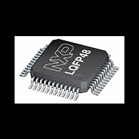
LPC1114FBD48 NXP Semiconductors, LPC1114FBD48 Datasheet - Page 81

LPC1114FBD48
Manufacturer Part Number
LPC1114FBD48
Description
The LPC1114FBD48 is an ARM Cortex-M0 microcontroller and it can operate up to 50 MHz
Manufacturer
NXP Semiconductors
Datasheet
1.LPC1110FD20.pdf
(103 pages)
Available stocks
Company
Part Number
Manufacturer
Quantity
Price
Company:
Part Number:
LPC1114FBD48
Manufacturer:
MARVELL
Quantity:
560
Part Number:
LPC1114FBD48
Manufacturer:
NXP/恩智浦
Quantity:
20 000
Company:
Part Number:
LPC1114FBD48/301
Manufacturer:
NXP
Quantity:
4
Part Number:
LPC1114FBD48/301
Manufacturer:
NXP/恩智浦
Quantity:
20 000
Company:
Part Number:
LPC1114FBD48/301,1
Manufacturer:
SAMSUNG
Quantity:
1 085
Company:
Part Number:
LPC1114FBD48/301,1
Manufacturer:
NXP Semiconductors
Quantity:
10 000
Company:
Part Number:
LPC1114FBD48/3011
Manufacturer:
NXP
Quantity:
5 000
Company:
Part Number:
LPC1114FBD48/301:1
Manufacturer:
NXP Semiconductors
Quantity:
10 000
Part Number:
LPC1114FBD48/302
Manufacturer:
NXP/恩智浦
Quantity:
20 000
Company:
Part Number:
LPC1114FBD48/302,1
Manufacturer:
NXP Semiconductors
Quantity:
10 000
Part Number:
LPC1114FBD48/303
Manufacturer:
NXP/恩智浦
Quantity:
20 000
NXP Semiconductors
11. Application information
LPC111X
Product data sheet
11.1 ADC usage notes
11.2 XTAL input
The following guidelines show how to increase the performance of the ADC in a noisy
environment beyond the ADC specifications listed in
The input voltage to the on-chip oscillators is limited to 1.8 V. If the oscillator is driven by a
clock in slave mode, it is recommended that the input be coupled through a capacitor with
C
capacitor to ground C
mode, a minimum of 200 mV (RMS) is needed.
In slave mode the input clock signal should be coupled by means of a capacitor of 100 pF
(Figure
corresponds to a square wave signal with a signal swing of between 280 mV and 1.4 V.
The XTALOUT pin in this configuration can be left unconnected.
External components and models used in oscillation mode are shown in
Table 26
and the capacitances C
fundamental mode oscillation (the fundamental frequency is represented by L, C
R
not be larger than 7 pF. Parameters F
manufacturer (see
Fig 43. Slave mode operation of the on-chip oscillator
•
•
•
•
i
S
= 100 pF. To limit the input voltage to the specified range, choose an additional
). Capacitance C
The ADC input trace must be short and as close as possible to the
LPC1110/11/12/13/14/15 chip.
The ADC input traces must be shielded from fast switching digital signals and noisy
power supply lines.
Because the ADC and the digital core share the same power supply, the power supply
line must be adequately filtered.
To improve the ADC performance in a very noisy environment, put the device in Sleep
mode during the ADC conversion.
43), with an amplitude between 200 mV (RMS) and 1000 mV (RMS). This
and
Table
All information provided in this document is subject to legal disclaimers.
Table
P
27. Since the feedback resistance is integrated on chip, only a crystal
in
g
which attenuates the input voltage by a factor C
Figure 44
X1
Rev. 7 — 1 March 2012
26).
and C
X2
represents the parallel package capacitance and should
need to be connected externally in case of
OSC
XTALIN
LPC1xxx
C i
100 pF
LPC1110/11/12/13/14/15
, C
L
, R
S
002aae788
32-bit ARM Cortex-M0 microcontroller
C g
and C
Table
P
are supplied by the crystal
15:
i
/(C
© NXP B.V. 2012. All rights reserved.
Figure 44
i
+ C
g
). In slave
L
81 of 103
and
and in


