LPC2290 NXP Semiconductors, LPC2290 Datasheet - Page 12

LPC2290
Manufacturer Part Number
LPC2290
Description
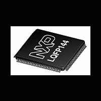
The LPC2290 microcontroller is based on a 16/32-bit ARM7TDMI-S CPU with real-timeemulation and embedded trace support
Manufacturer
NXP Semiconductors
Datasheet
1.LPC2290.pdf
(41 pages)
Available stocks
Company
Part Number
Manufacturer
Quantity
Price
Company:
Part Number:
LPC2290FBD/01
Manufacturer:
OTI
Quantity:
8
Company:
Part Number:
LPC2290FBD144
Manufacturer:
MIT
Quantity:
90
Company:
Part Number:
LPC2290FBD144,551
Manufacturer:
NXP Semiconductors
Quantity:
10 000
Company:
Part Number:
LPC2290FBD144/01
Manufacturer:
NXP
Quantity:
50 000
Company:
Part Number:
LPC2290FBD144/01,5
Manufacturer:
NXP Semiconductors
Quantity:
10 000
Company:
Part Number:
LPC2290FBD144/015
Manufacturer:
NXP Semiconductors
Quantity:
135
NXP Semiconductors
Table 3.
LPC2290_3
Product data sheet
Symbol
P3.20/A20
P3.21/A21
P3.22/A22
P3.23/A23/
XCLK
P3.24/CS3
P3.25/CS2
P3.26/CS1
P3.27/WE
P3.28/BLS3/
AIN7
P3.29/BLS2/
AIN6
P3.30/BLS1
P3.31/BLS0
TD1
RESET
XTAL1
XTAL2
V
V
SS
SSA
Pin description
Pin
45
44
41
40
36
35
30
29
28
27
97
96
22
135
142
141
3, 9, 26, 38,
54, 67, 79,
93, 103, 107,
111, 128
139
[5]
[5]
[5]
[5]
[5]
[5]
[5]
[5]
[2]
[4]
[4]
[4]
[5]
[6]
[7]
[7]
…continued
Type
I/O
O
I/O
O
I/O
O
I/O
I/O
O
I/O
O
I/O
O
I/O
O
I/O
O
I/O
O
I
I/O
O
I
I/O
O
I/O
O
O
I
I
O
I
I
Description
P3.20 — General purpose digital input/output pin.
A20 — External memory address line 20.
P3.21 — General purpose digital input/output pin.
A21 — External memory address line 21.
P3.22 — General purpose digital input/output pin.
A22 — External memory address line 22.
P3.23 — General purpose digital input/output pin.
A23 — External memory address line 23.
XCLK — Clock output.
P3.24 — General purpose digital input/output pin.
CS3 — LOW-active Chip Select 3 signal.
(Bank 3 addresses range 0x8300 0000 to 0x83FF FFFF)
P3.25 — General purpose digital input/output pin.
CS2 — LOW-active Chip Select 2 signal.
(Bank 2 addresses range 0x8200 0000 to 0x82FF FFFF)
P3.26 — General purpose digital input/output pin.
CS1 — LOW-active Chip Select 1 signal.
(Bank 1 addresses range 0x8100 0000 to 0x81FF FFFF)
P3.27 — General purpose digital input/output pin.
WE — LOW-active Write enable signal.
P3.28 — General purpose digital input/output pin.
BLS3 — LOW-active Byte Lane Select signal (Bank 3).
AIN7 — ADC, input 7. This analog input is always connected to its pin.
P3.29 — General purpose digital input/output pin.
BLS2 — LOW-active Byte Lane Select signal (Bank 2).
AIN6 — ADC, input 6. This analog input is always connected to its pin.
P3.30 — General purpose digital input/output pin.
BLS1 — LOW-active Byte Lane Select signal (Bank 1).
P3.31 — General purpose digital input/output pin.
BLS0 — LOW-active Byte Lane Select signal (Bank 0).
TD1: CAN1 transmitter output.
External Reset input: A LOW on this pin resets the device, causing I/O ports
and peripherals to take on their default states, and processor execution to
begin at address 0. TTL with hysteresis, 5 V tolerant.
Input to the oscillator circuit and internal clock generator circuits.
Output from the oscillator amplifier.
Ground: 0 V reference.
Analog ground: 0 V reference. This should nominally be the same voltage
as V
Rev. 03 — 16 November 2006
SS
16/32-bit ARM microcontroller with external memory interface
, but should be isolated to minimize noise and error.
LPC2290
© NXP B.V. 2006. All rights reserved.
12 of 41


