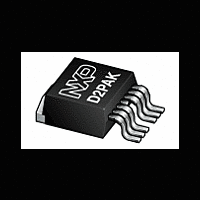
BUK6C2R1-55C NXP Semiconductors, BUK6C2R1-55C Datasheet - Page 8

BUK6C2R1-55C
Manufacturer Part Number
BUK6C2R1-55C
Description
Intermediate level gate drive N-channel enhancement mode Field-Effect Transistor (FET) in a plastic package using TrenchMOS technology
Manufacturer
NXP Semiconductors
Datasheet
1.BUK6C2R1-55C.pdf
(13 pages)
NXP Semiconductors
BUK6C2R1-55C
Product data sheet
Fig 13. Gate-source voltage as a function of gate
Fig 15. Input, output and reverse transfer capacitances
(pF)
V
C
(V)
10
GS
10
10
10
10
5
4
3
2
8
6
4
2
0
10
charge; typical values
as a function of drain-source voltage; typical
values
T
V
0
-1
j
GS
V
= 25 °C; I
DS
= 0 V; f = 1 MHz
= 44V
D
100
= 180 A
1
200
10
Q
V
All information provided in this document is subject to legal disclaimers.
G
DS
003aaf970
(nC)
003aaf973
(V)
C
C
C
oss
rss
iss
10
300
Rev. 3 — 18 January 2012
2
Fig 14. Gate charge waveform definitions
Fig 16. Source (diode forward) current as a function of
(A)
I
S
300
200
100
N-channel TrenchMOS intermediate level FET
0
source-drain (diode forward) voltage; typical
values
V
0
V
GS
V
V
V
GS(pl)
DS
GS(th)
GS
= 0 V
T
j
= 175 ° C
Q
GS1
0.5
I
Q
D
BUK6C2R1-55C
GS
Q
GS2
Q
G(tot)
T
Q
j
GD
= 25 ° C
1
© NXP B.V. 2012. All rights reserved.
V
SD
003aaa508
003aaf974
(V)
1.5
8 of 13


