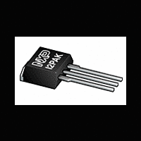
PSMN1R1-30EL NXP Semiconductors, PSMN1R1-30EL Datasheet - Page 2

PSMN1R1-30EL
Manufacturer Part Number
PSMN1R1-30EL
Description
Manufacturer
NXP Semiconductors
Datasheet
1.PSMN1R1-30EL.pdf
(14 pages)
NXP Semiconductors
2. Pinning information
Table 2.
3. Ordering information
Table 3.
PSMN1R1-30EL
Product data sheet
Pin
1
2
3
mb
Type number
PSMN1R1-30EL
Symbol Description
G
D
S
D
Pinning information
Ordering information
gate
drain
source
mounting base; connected to
drain
Table 1.
[1]
[2]
Package
Name
I2PAK
Symbol
Dynamic characteristics
Q
Q
Avalanche ruggedness
E
DS(AL)S
GD
G(tot)
Continuous current is limited by package.
Measured 3 mm from package.
Quick reference data
Parameter
gate-drain charge V
total gate charge
non-repetitive
drain-source
avalanche energy
Description
plastic single-ended package (I2PAK); TO-262
All information provided in this document is subject to legal disclaimers.
Rev. 2 — 15 April 2011
Simplified outline
SOT226 (I2PAK)
Conditions
V
see
V
I
R
D
…continued
GS
DS
GS
GS
= 120 A; V
N-channel 30 V 1.3 mΩ logic level MOSFET in I2PAK
Figure 15
= 4.5 V; I
= 15 V; see
= 10 V; T
= 50 Ω; unclamped
1
mb
2
3
sup
D
j(init)
= 75 A;
≤ 30 V;
Figure
= 25 °C;
14;
Graphic symbol
PSMN1R1-30EL
mbb076
G
Min
-
-
-
© NXP B.V. 2011. All rights reserved.
D
S
Typ
37
118
-
SOT226
Version
Max Unit
-
-
1.9
2 of 14
nC
nC
J


