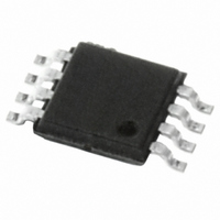
STVM100DS6F STMicroelectronics, STVM100DS6F Datasheet - Page 10

STVM100DS6F
Manufacturer Part Number
STVM100DS6F
Description
IC I2C LCD VCOM CALIBRATR 8TSSOP
Manufacturer
STMicroelectronics
Type
Calibratorr
Datasheet
1.STVM100DS6F.pdf
(27 pages)
Specifications of STVM100DS6F
Applications
TFT-LCD Panels: VCOM Driver
Mounting Type
Surface Mount
Package / Case
8-TSSOP
Lead Free Status / RoHS Status
Lead free / RoHS Compliant
Other names
497-9082-2
STVM100DS6F
STVM100DS6F
Available stocks
Company
Part Number
Manufacturer
Quantity
Price
Part Number:
STVM100DS6F
Manufacturer:
ST
Quantity:
20 000
Device operation
2.2
2.3
2.4
10/27
Read mode
In READ mode, after the start condition, the master sets the slave address (see
Followed by the READ/WRITE mode control bit (R/W=1) and the acknowledge bit, the value
in DAC register will be transmitted and the master receiver will send an acknowledge bit to
the slave transmitter. Finally the stop condition will terminate the READ operation. In READ
mode, the valid data is the first 7 bits and the P bit (the eight bit) is don’t care.
Write mode
In WRITE mode the master transmits to the STVM100 slave receiver. The bus protocol is
shown in
placed on the bus to identify a WRITE operation. After the acknowledgement by the slave,
the data will be transmitted to the slave with the 7-bit which indicates the data is valid as well
as the eighth bit “P” for the register’s identification. When P = 1, the DAC register is written
to, and when P = 0, the EEPROM is written to (Programming). After receiving the data, the
slave will generate an acknowledge signal, then a stop condition will terminate the WRITE
operation. STVM100 is pre-programmed with 80H in the EEPROM after manufacturing.
A period of t
slave will not acknowledge any WRITE operation.
The bit P values in both READ and WRITE modes are shown in
Figure 7.
Table 3.
V
The ramp-up from 10% V
10ms to ensure that the EEPROM and power-on reset circuits are synchronized, and the
correct value is read from the EEPROM.
DD
power supply ramp-up
Figure
SDA
SCL
Operation
WRITE
W
READ
Read/write mode sequence
Bit P read and write mode values
(see
START
7. Following the start condition and slave address, a logic '0' (R/W = 0) is
START
Table
1
1
0
0
SLAVE ADDRESS
DD
8) is needed for EEPROM programming. During this period, the
0
0
1
1
to 90% V
Doc ID 13236 Rev 7
1
1
1
1
1
1
DD
R/W A
R/W
P-bit value
level should be achieved in less than or equal to
A
X
1
0
6
6
5
5
4
4
3
3
2
2
1
1
0
Table
0
P
DAC register WRITE
P
EEPROM WRITE
A
(programming)
A
3.
STOP
Description
Don’t care
STOP
Figure
STVM100
AI12276_b
7).


