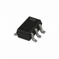
74AUP2G17GW,125 NXP Semiconductors, 74AUP2G17GW,125 Datasheet - Page 12

74AUP2G17GW,125
Manufacturer Part Number
74AUP2G17GW,125
Description
IC BUFF DL SCHM TRG L PWR SC88
Manufacturer
NXP Semiconductors
Series
74AUPr
Datasheet
1.74AUP2G17GM115.pdf
(21 pages)
Specifications of 74AUP2G17GW,125
Package / Case
SC-70-6, SC-88, SOT-363
Logic Type
Schmitt Trigger - Buffer, Driver
Number Of Elements
2
Number Of Bits Per Element
1
Current - Output High, Low
4mA, 4mA
Voltage - Supply
0.8 V ~ 3.6 V
Operating Temperature
-40°C ~ 125°C
Mounting Type
Surface Mount
Logic Family
AUP
Number Of Channels Per Chip
2
Polarity
Non-Inverting
Supply Voltage (max)
3.6 V
Supply Voltage (min)
0.8 V
Maximum Operating Temperature
+ 125 C
Mounting Style
SMD/SMT
High Level Output Current
- 4 mA
Input Bias Current (max)
0.5 uA
Low Level Output Current
4 mA
Minimum Operating Temperature
- 40 C
Propagation Delay Time
19 ns @ 1.1 V to 1.3 V or 11.2 ns @ 1.4 V to 1.6 V or 9.2 ns @ 1.65 V to 1.95 V or 7 ns @ 2.3 V to 2.7 V or 6.2 ns @ 3 V to 3.6 V
Number Of Lines (input / Output)
2 / 2
Lead Free Status / RoHS Status
Lead free / RoHS Compliant
Lead Free Status / RoHS Status
Lead free / RoHS Compliant, Lead free / RoHS Compliant
Other names
74AUP2G17GW-G
74AUP2G17GW-G
935279991125
74AUP2G17GW-G
935279991125
NXP Semiconductors
15. Application information
74AUP2G17
Product data sheet
The slow input rise and fall times cause additional power dissipation, this can be
calculated using the following formula:
P
Average ΔI
Fig 13. Average I
add
P
f
t
t
ΔI
i
r
f
add
= input frequency (MHz);
= input fall time (ns); 90 % to 10 %;
= input rise time (ns); 10 % to 90 %;
CC(AV)
= f
(1) Positive-going edge.
(2) Negative-going edge.
= additional power dissipation (μW);
i
× (t
Linear change of V
specified.
= average additional supply current (μA).
CC(AV)
r
× ΔI
All information provided in this document is subject to legal disclaimers.
CC(AV)
differs with positive or negative input transitions, as shown in
CC
ΔI
(mA)
CC(AV)
as a function of V
Rev. 4 — 3 November 2010
+ t
0.3
0.2
0.1
I
0
0.8
between 0.8 V and 2.0 V. All values given are typical, unless otherwise
f
× ΔI
CC(AV)
) × V
1.8
CC
CC
where:
2.8
V
(1)
(2)
CC
Low-power dual Schmitt trigger
001aad027
(V)
3.8
74AUP2G17
© NXP B.V. 2010. All rights reserved.
Figure
12 of 21
13.


