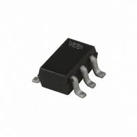
74AUP2G17GW,125 NXP Semiconductors, 74AUP2G17GW,125 Datasheet - Page 7

74AUP2G17GW,125
Manufacturer Part Number
74AUP2G17GW,125
Description
IC BUFF DL SCHM TRG L PWR SC88
Manufacturer
NXP Semiconductors
Series
74AUPr
Datasheet
1.74AUP2G17GM115.pdf
(21 pages)
Specifications of 74AUP2G17GW,125
Package / Case
SC-70-6, SC-88, SOT-363
Logic Type
Schmitt Trigger - Buffer, Driver
Number Of Elements
2
Number Of Bits Per Element
1
Current - Output High, Low
4mA, 4mA
Voltage - Supply
0.8 V ~ 3.6 V
Operating Temperature
-40°C ~ 125°C
Mounting Type
Surface Mount
Logic Family
AUP
Number Of Channels Per Chip
2
Polarity
Non-Inverting
Supply Voltage (max)
3.6 V
Supply Voltage (min)
0.8 V
Maximum Operating Temperature
+ 125 C
Mounting Style
SMD/SMT
High Level Output Current
- 4 mA
Input Bias Current (max)
0.5 uA
Low Level Output Current
4 mA
Minimum Operating Temperature
- 40 C
Propagation Delay Time
19 ns @ 1.1 V to 1.3 V or 11.2 ns @ 1.4 V to 1.6 V or 9.2 ns @ 1.65 V to 1.95 V or 7 ns @ 2.3 V to 2.7 V or 6.2 ns @ 3 V to 3.6 V
Number Of Lines (input / Output)
2 / 2
Lead Free Status / RoHS Status
Lead free / RoHS Compliant
Lead Free Status / RoHS Status
Lead free / RoHS Compliant, Lead free / RoHS Compliant
Other names
74AUP2G17GW-G
74AUP2G17GW-G
935279991125
74AUP2G17GW-G
935279991125
NXP Semiconductors
11. Dynamic characteristics
Table 8.
Voltages are referenced to GND (ground = 0 V); for test circuit see
74AUP2G17
Product data sheet
Symbol Parameter
C
t
C
t
C
t
C
t
pd
pd
pd
pd
L
L
L
L
= 5 pF
= 10 pF
= 15 pF
= 30 pF
propagation delay nA to nY; see
propagation delay nA to nY; see
propagation delay nA to nY; see
propagation delay nA to nY; see
Dynamic characteristics
Conditions
V
V
V
V
V
V
V
V
V
V
V
V
V
V
V
V
V
V
V
V
V
V
V
V
CC
CC
CC
CC
CC
CC
CC
CC
CC
CC
CC
CC
CC
CC
CC
CC
CC
CC
CC
CC
CC
CC
CC
CC
= 0.8 V
= 1.1 V to 1.3 V
= 1.4 V to 1.6 V
= 1.65 V to 1.95 V
= 2.3 V to 2.7 V
= 3.0 V to 3.6 V
= 0.8 V
= 1.1 V to 1.3 V
= 1.4 V to 1.6 V
= 1.65 V to 1.95 V
= 2.3 V to 2.7 V
= 3.0 V to 3.6 V
= 0.8 V
= 1.1 V to 1.3 V
= 1.4 V to 1.6 V
= 1.65 V to 1.95 V
= 2.3 V to 2.7 V
= 3.0 V to 3.6 V
= 0.8 V
= 1.1 V to 1.3 V
= 1.4 V to 1.6 V
= 1.65 V to 1.95 V
= 2.3 V to 2.7 V
= 3.0 V to 3.6 V
All information provided in this document is subject to legal disclaimers.
Figure 7
Figure 7
Figure 7
Figure 7
Rev. 4 — 3 November 2010
[2]
[2]
[2]
[2]
Figure 8
Min
2.6
2.4
1.9
1.8
2.9
2.6
2.3
2.1
3.2
3.1
2.6
2.5
3.9
3.4
3.3
2.0
2.5
2.7
3.5
3.5
-
-
-
-
25 °C
Typ
19.0
22.5
26.0
36.3
5.7
4.2
3.6
3.0
2.7
6.6
4.8
4.2
3.5
3.3
7.4
5.4
4.7
4.0
3.7
9.7
7.0
6.0
5.1
4.8
[1]
Max
10.6
12.4
14.1
19.0
11.2
6.5
5.5
4.2
3.6
7.8
6.3
4.8
4.4
8.7
7.1
5.6
4.9
9.2
7.0
6.2
-
-
-
-
Low-power dual Schmitt trigger
Min
2.5
2.3
1.9
1.8
1.5
2.7
2.4
2.4
2.1
2.0
3.1
2.8
2.7
2.5
2.2
3.7
3.6
3.4
3.2
3.1
-
-
-
-
−40 °C to +125 °C
74AUP2G17
(85 °C)
Max
10.9
12.9
14.7
19.8
12.4
10.1
7.1
6.1
4.6
3.8
8.3
6.8
5.3
4.6
9.5
7.8
6.0
5.2
7.5
7.1
-
-
-
-
© NXP B.V. 2010. All rights reserved.
(125 °C)
Max
11.1
13.0
14.9
20.1
13.0
10.7
7.4
6.3
4.8
4.0
8.7
7.1
5.6
4.8
9.9
8.2
6.3
5.5
7.9
7.5
-
-
-
-
7 of 21
Unit
ns
ns
ns
ns
ns
ns
ns
ns
ns
ns
ns
ns
ns
ns
ns
ns
ns
ns
ns
ns
ns
ns
ns
ns


