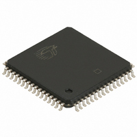
CY7C4275-10ASC Cypress Semiconductor Corp, CY7C4275-10ASC Datasheet - Page 4

CY7C4275-10ASC
Manufacturer Part Number
CY7C4275-10ASC
Description
IC DEEP SYN FIFO 32KX18 64LQFP
Manufacturer
Cypress Semiconductor Corp
Series
CY7Cr
Datasheet
1.CY7C4275-10ASC.pdf
(21 pages)
Specifications of CY7C4275-10ASC
Function
Synchronous
Memory Size
576K (32K x 18)
Data Rate
100MHz
Access Time
8ns
Voltage - Supply
3.3V
Operating Temperature
-40°C ~ 85°C
Mounting Type
Surface Mount
Package / Case
64-LQFP
Lead Free Status / RoHS Status
Contains lead / RoHS non-compliant
Other names
428-1239
Available stocks
Company
Part Number
Manufacturer
Quantity
Price
Company:
Part Number:
CY7C4275-10ASC
Manufacturer:
Cypress Semiconductor Corp
Quantity:
10 000
Maximum Ratings
(Above which the useful life may be impaired. For user guide-
lines, not tested.)
Storage Temperature ................................–65 C to +150 C
Ambient Temperature with
Power Applied............................................–55 C to +125 C
Supply Voltage to Ground Potential ............... –0.5V to +7.0V
DC Voltage Applied to Outputs
in High Z State ............................................... –0.5V to +7.0V
DC Input Voltage
Electrical Characteristics
Capacitance
Notes:
Document #: 38-06008 Rev. *A
1.
2.
3.
4.
5.
6.
7.
8.
V
V
V
V
I
I
I
I
I
C
C
IX
OZL
OZH
CC1
SB
Parameter
OH
OL
IH
IL
IN
OUT
[5]
[7]
The Voltage on any input or I/O pin cannot exceed the power pin during power-up.
T
See the last page of this specification for Group A subgroup testing information.
The V
previous device or V
The V
previous device or V
Input signals switch from 0V to 3V with a rise/fall time of less than 3 ns, clocks and clock enables switch at 20 MHz, while data inputs switch at 10 MHz. Outputs
are unloaded. Icc1(typical) = (25 mA+(freq –20MHz)*(1.0 mA/MHz)).
All inputs = V
Tested initially and after any design changes that may affect these parameters.
[4]
A
[6]
is the “instant on” case temperature.
Parameter
IH
IH
and V
and V
CC
IL
IL
[8]
Output HIGH Voltage
Output LOW Voltage
Input HIGH Voltage
Input LOW Voltage
Input Leakage
Current
Output OFF,
High Z Current
Active Power Supply
Current
Average Standby
Current
– 0.2V, except RCLK and WCLK (which are at frequency = 0 MHz), and FL/RT which is at V
specifications apply for all inputs except WXI, RXI. The WXI, RXI pin is not a TTL input. It is connected to either RXO, WXO of the
specifications apply for all inputs except WXI, RXI. The WXI, RXI pin is not a TTL input. It is connected to either RXO, WXO of the
SS
SS.
.
Description
[1]
Input Capacitance
Output Capacitance
Over the Operating Range
Description
0.5V to V
V
I
V
I
V
OE > V
V
OH
OL
CC
CC
CC
SS
Test Conditions
= 8.0 mA
= –2.0 mA
< V
= Max.
= Min.,
= Min.,
CC
IH
O
,
+0.5V
< V
CC
T
V
A
CC
Com’l
Ind
Com’l
Ind
= 25 C, f = 1 MHz,
[3]
= 5.0V
Test Conditions
Output Current into Outputs (LOW)............................. 20 mA
Static Discharge Voltage............................................ >2001V
(per MIL–STD–883, Method 3015)
Latch-Up Current..................................................... >200 mA
Operating Range
Commercial
Industrial
Min.
–0.5
Range
–10
–10
7C42X5-10
2.4
2.0
[2]
Max.
V
+10
+10
0.4
0.8
50
55
CC
2
2
Min.
–0.5
–10
–10
2.4
2.0
–40 C to +85 C
7C42X5-5
0 C to +70 C
Temperature
SS
Ambient
. All outputs are unloaded.
Max.
V
+10
+10
0.4
0.8
50
2
Max.
CC
5
7
Min.
–0.5
–10
–10
7C42X5-25
2.4
2.0
CY7C4275
CY7C4285
Max.
V
+10
+10
0.4
0.8
50
5V
5V
CC
2
Page 4 of 21
Unit
V
pF
pF
CC
10%
10%
Unit
mA
mA
mA
mA
V
V
V
V
A
A


