74HC74PW,118 NXP Semiconductors, 74HC74PW,118 Datasheet - Page 9
74HC74PW,118
Manufacturer Part Number
74HC74PW,118
Description
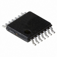
IC DUAL POS-EDG-TRG D FF 14TSSOP
Manufacturer
NXP Semiconductors
Series
74HCr
Type
D-Typer
Datasheet
1.74HC74BQ115.pdf
(22 pages)
Specifications of 74HC74PW,118
Output Type
Differential
Package / Case
14-TSSOP
Function
Set(Preset) and Reset
Number Of Elements
2
Number Of Bits Per Element
1
Frequency - Clock
82MHz
Delay Time - Propagation
14ns
Trigger Type
Positive Edge
Current - Output High, Low
5.2mA, 5.2mA
Voltage - Supply
2 V ~ 6 V
Operating Temperature
-40°C ~ 125°C
Mounting Type
Surface Mount
Number Of Circuits
2
Logic Family
HC
Logic Type
D-Type Edge Triggered Flip-Flop
Polarity
Inverting/Non-Inverting
Input Type
Single-Ended
Propagation Delay Time
14 ns at 5 V
High Level Output Current
- 5.2 mA
Low Level Output Current
5.2 mA
Supply Voltage (max)
6 V
Maximum Operating Temperature
+ 125 C
Mounting Style
SMD/SMT
Minimum Operating Temperature
- 40 C
Supply Voltage (min)
2 V
Lead Free Status / RoHS Status
Lead free / RoHS Compliant
Lead Free Status / RoHS Status
Lead free / RoHS Compliant, Lead free / RoHS Compliant
Other names
568-4574-2
74HC74PW-T
74HC74PW-T
935175130118
74HC74PW-T
74HC74PW-T
935175130118
Available stocks
Company
Part Number
Manufacturer
Quantity
Price
Company:

Part Number:
74HC74PW,118
Manufacturer:
NXP Semiconductors
Quantity:
1 950


Philips Semiconductors
Family 74HCT
At recommended operating conditions; voltages are referenced to GND (ground = 0 V).
Note
1. All typical values are measured at T
Remark to HCT types
The value of additional quiescent supply current ( I
multiply this value by the unit load coefficient shown in the table.
2003 Jul 10
T
V
V
V
V
I
I
T
V
V
V
V
I
I
LI
CC
LI
CC
amb
I
amb
I
IH
IL
OH
OL
IH
IL
OH
OL
Dual D-type flip-flop with set and reset;
positive-edge trigger
CC
CC
SYMBOL
= 40 to +85 C; note 1
= 40 to +125 C
HIGH-level input
voltage
LOW-level input voltage
HIGH-level output
voltage
LOW-level output
voltage
input leakage current
quiescent supply
current
additional quiescent
supply current per input
HIGH-level input
voltage
LOW-level input voltage
HIGH-level output
voltage
LOW-level output
voltage
input leakage current
quiescent supply
current
additional quiescent
supply current per input
PARAMETER
INPUT
nRD
nSD
nCP
nD
amb
V
I
V
I
V
V
I
V
inputs at V
I
V
I
V
I
V
V
I
V
inputs at V
I
O
O
O
O
O
O
O
O
I
I
I
I
I
I
I
I
I
I
= 25 C.
= V
= 4.0 mA
= V
= 4.0 mA
= V
= V
= 0
= V
= 0
= V
= 4.0 mA
= V
= 4.0 mA
= V
= V
= 0
= V
= 0
WAVEFORMS
IH
IH
CC
CC
CC
IH
IH
CC
CC
CC
TEST CONDITIONS
or V
or V
or V
or V
or GND
or GND;
or GND
or GND;
CC
2.1 V other
2.1 V other
CC
CC
) for a unit load of 1 is given here. To determine I
IL
IL
IL
IL
or GND;
or GND;
;
;
;
;
9
4.5 to 5.5 2.0
4.5 to 5.5
4.5
4.5
5.5
5.5
4.5 to 5.5
4.5 to 5.5 2.0
4.5 to 5.5
4.5
4.5
5.5
5.5
4.5 to 5.5
V
CC
(V)
UNIT LOAD COEFFICIENT
3.84
0.33
3.7
MIN.
0.70
0.70
0.80
0.80
74HC74; 74HCT74
1.6
1.2
4.32
0.15
100
TYP.
Product specification
0.8
40
450
0.8
0.4
80
490
1.0
1.0
MAX.
CC
per input,
V
V
V
V
V
V
V
V
A
A
A
A
A
A
UNIT
Related parts for 74HC74PW,118
Image
Part Number
Description
Manufacturer
Datasheet
Request
R

Part Number:
Description:
IC DUAL POS-EDG-TRG D FF 14TSSOP
Manufacturer:
NXP Semiconductors
Datasheet:

Part Number:
Description:
Flip Flops DUAL D-TYPE POSITIVE EDGE-TRIG
Manufacturer:
NXP Semiconductors
Datasheet:
Part Number:
Description:
Flip Flop D-Type Pos-Edge 2-Element 14-Pin TSSOP T/R
Manufacturer:
NXP Semiconductors
Datasheet:
Part Number:
Description:
NXP Semiconductors designed the LPC2420/2460 microcontroller around a 16-bit/32-bitARM7TDMI-S CPU core with real-time debug interfaces that include both JTAG andembedded trace
Manufacturer:
NXP Semiconductors
Datasheet:

Part Number:
Description:
NXP Semiconductors designed the LPC2458 microcontroller around a 16-bit/32-bitARM7TDMI-S CPU core with real-time debug interfaces that include both JTAG andembedded trace
Manufacturer:
NXP Semiconductors
Datasheet:
Part Number:
Description:
NXP Semiconductors designed the LPC2468 microcontroller around a 16-bit/32-bitARM7TDMI-S CPU core with real-time debug interfaces that include both JTAG andembedded trace
Manufacturer:
NXP Semiconductors
Datasheet:
Part Number:
Description:
NXP Semiconductors designed the LPC2470 microcontroller, powered by theARM7TDMI-S core, to be a highly integrated microcontroller for a wide range ofapplications that require advanced communications and high quality graphic displays
Manufacturer:
NXP Semiconductors
Datasheet:
Part Number:
Description:
NXP Semiconductors designed the LPC2478 microcontroller, powered by theARM7TDMI-S core, to be a highly integrated microcontroller for a wide range ofapplications that require advanced communications and high quality graphic displays
Manufacturer:
NXP Semiconductors
Datasheet:
Part Number:
Description:
The Philips Semiconductors XA (eXtended Architecture) family of 16-bit single-chip microcontrollers is powerful enough to easily handle the requirements of high performance embedded applications, yet inexpensive enough to compete in the market for hi
Manufacturer:
NXP Semiconductors
Datasheet:
Part Number:
Description:
The XA-S3 device is a member of Philips Semiconductors? XA(eXtended Architecture) family of high performance 16-bitsingle-chip microcontrollers
Manufacturer:
NXP Semiconductors
Datasheet:

Part Number:
Description:
The NXP BlueStreak LH75401/LH75411 family consists of two low-cost 16/32-bit System-on-Chip (SoC) devices
Manufacturer:
NXP Semiconductors
Datasheet:
Part Number:
Description:
The NXP LPC3130/3131 combine an 180 MHz ARM926EJ-S CPU core, high-speed USB2
Manufacturer:
NXP Semiconductors
Datasheet:
Part Number:
Description:
The NXP LPC3141 combine a 270 MHz ARM926EJ-S CPU core, High-speed USB 2
Manufacturer:
NXP Semiconductors
Part Number:
Description:
The NXP LPC3143 combine a 270 MHz ARM926EJ-S CPU core, High-speed USB 2
Manufacturer:
NXP Semiconductors