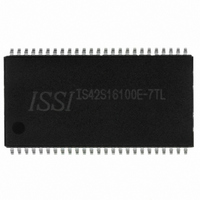
IS42S16100E-7TL ISSI, Integrated Silicon Solution Inc, IS42S16100E-7TL Datasheet - Page 7

IS42S16100E-7TL
Manufacturer Part Number
IS42S16100E-7TL
Description
IC SDRAM 16MBIT 143MHZ 50TSOP
Manufacturer
ISSI, Integrated Silicon Solution Inc
Type
SDRAMr
Specifications of IS42S16100E-7TL
Format - Memory
RAM
Memory Type
SDRAM
Memory Size
16M (1M x 16)
Speed
143MHz
Interface
Parallel
Voltage - Supply
3 V ~ 3.6 V
Operating Temperature
0°C ~ 70°C
Package / Case
50-TSOPII
Organization
1Mx16
Density
16Mb
Address Bus
12b
Access Time (max)
6/5.5ns
Maximum Clock Rate
143MHz
Operating Supply Voltage (typ)
3.3V
Package Type
TSOP-II
Operating Temp Range
0C to 70C
Operating Supply Voltage (max)
3.6V
Operating Supply Voltage (min)
3V
Supply Current
130mA
Pin Count
50
Mounting
Surface Mount
Operating Temperature Classification
Commercial
Lead Free Status / RoHS Status
Lead free / RoHS Compliant
Other names
706-1071
IS42S16100E-7TL
IS42S16100E-7TL
Available stocks
Company
Part Number
Manufacturer
Quantity
Price
Company:
Part Number:
IS42S16100E-7TL
Manufacturer:
ISSI
Quantity:
6 545
Company:
Part Number:
IS42S16100E-7TL
Manufacturer:
ISSI
Quantity:
851
Company:
Part Number:
IS42S16100E-7TLI
Manufacturer:
ISSI
Quantity:
11 200
Company:
Part Number:
IS42S16100E-7TLI
Manufacturer:
ISSI
Quantity:
104
Part Number:
IS42S16100E-7TLI
Manufacturer:
ISSI
Quantity:
20 000
IS42S16100E, IC42S16100E
AC CHARACTERISTICS
Symbol Parameter
Notes:
1. When power is first applied, memory operation should be started 100 µs after V
2. measured with t
3. The reference level is 1.4 V when measuring input signal timing. Rise and fall times are measured between V
4. Access time is measured at 1.4V with the load shown in the figure below.
5. The time t
Integrated Silicon Solution, Inc. — www.issi.com
Rev. C
01/22/08
t
t
t
t
t
t
t
t
t
t
t
t
t
t
t
t
t
t
t
t
t
t
t
t
t
t
t
t
t
t
t
ck
ck
ac
ac
chi
cl
oh
oh
lz
hz
hz
ds
dh
as
ah
cks
ckh
cka
cs
ch
rc
ras
rp
rcd
rrd
dpl
dpl
dal
dal
t
ref
sequence must be executed before starting memory operation.
output is in the high impedance state.
3
2
3
2
3
2
3
2
3
2
3
2
hz
Clock Cycle Time
Access Time From CLK
CLK HIGH Level Width
CLK LOW Level Width
Output Data Hold Time
Output LOW Impedance Time
Output HIGH Impedance Time
Input Data Setup Time
Input Data Hold Time
Address Setup Time
Address Hold Time
CKE Setup Time
CKE Hold Time
CKE to CLK Recovery Delay Time
Command Setup Time (CS, RAS, CAS, WE, DQM)
Command Hold Time (CS, RAS, CAS, WE, DQM)
Command Period (REF to REF / ACT to ACT)
Command Period (ACT to PRE)
Command Period (PRE to ACT)
Active Command To Read / Write Command Delay Time
Command Period (ACT [0] to ACT[1])
Input Data To Precharge
Command Delay time
Input Data To Active / Refresh
Command Delay time (During Auto-Precharge)
Transition Time
Refresh Cycle Time (2048)
(max.) is defined as the time required for the output voltage to transition by ± 200 mV from V
t
= 1 ns.
(4)
(1,2,3)
(5)
CAS Latency = 3
CAS Latency = 2
CAS Latency = 3
CAS Latency = 2
CAS Latency = 3
CAS Latency = 2
CAS Latency = 3
CAS Latency = 2
CAS Latency = 3
CAS Latency = 2
CAS Latency = 3
CAS Latency = 2
dd
and V
ddq
2CLK+t
2CLK+t
1CLK+3 —
reach their stipulated voltages. Also note that the power-on
Min. Max.
2.5
48
32
16
16
—
—
—
—
11
—
—
—
5
8
2
2
2
0
2
1
2
1
2
1
2
1
1
-5
rp
rp
2CLK
2CLK
10
32
—
—
—
—
—
—
—
—
—
—
—
—
—
—
—
—
—
—
—
—
—
—
5
6
4
6
oh
(min.) or V
ih
(min.) and V
2CLK+t
2CLK+t
1CLK+3
2CLK
2CLK
Min.
2.5
2.5
2.0
2.5
54
36
18
16
12
—
—
—
—
—
6
8
0
2
1
2
1
2
1
2
1
1
ol
rp
rp
(max.) when the
-6
100,000
il
Max.
(max.).
5.5
5.5
—
—
—
—
—
—
—
—
—
—
—
—
—
—
—
—
—
—
—
—
—
—
—
—
10
32
6
6
2CLK+t
2CLK+t
1CLK+3
2CLK
2CLK
Min.
2.5
2.5
2.0
2.5
63
42
20
16
14
—
—
—
—
—
7
8
0
2
1
2
1
2
1
2
1
1
rp
rp
-7
100,000
Max.
5.5
5.5
10
32
—
—
—
—
—
—
—
—
—
—
—
—
—
—
—
—
—
—
—
—
—
—
—
—
6
6
Units
ms
ns
ns
ns
ns
ns
ns
ns
ns
ns
ns
ns
ns
ns
ns
ns
ns
ns
ns
ns
ns
ns
ns
ns
ns
ns
ns
ns
ns
ns
ns
7


