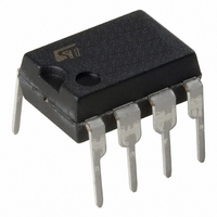
M24C02-WBN6P STMicroelectronics, M24C02-WBN6P Datasheet - Page 13

M24C02-WBN6P
Manufacturer Part Number
M24C02-WBN6P
Description
IC EEPROM 2KBIT 400KHZ 8DIP
Manufacturer
STMicroelectronics
Datasheets
1.M24C01-WMN6TP.pdf
(39 pages)
2.M24C02-WBN6P.pdf
(10 pages)
3.M24C02-WBN6P.pdf
(28 pages)
Specifications of M24C02-WBN6P
Format - Memory
EEPROMs - Serial
Memory Type
EEPROM
Memory Size
2K (256 x 8)
Speed
400kHz
Interface
I²C, 2-Wire Serial
Voltage - Supply
2.5 V ~ 5.5 V
Operating Temperature
-40°C ~ 85°C
Package / Case
8-DIP (0.300", 7.62mm)
Organization
256 K x 8
Interface Type
I2C
Maximum Clock Frequency
0.4 MHz
Access Time
900 ns
Supply Voltage (max)
5.5 V
Supply Voltage (min)
2.5 V
Maximum Operating Current
2 mA
Maximum Operating Temperature
+ 85 C
Mounting Style
Through Hole
Minimum Operating Temperature
- 40 C
Operating Supply Voltage
6.5 V
Capacitance, Input
8 pF (SDA), 6 pF (Other Pins)
Current, Input, Leakage
±2 μA
Current, Operating
2 mA
Current, Output, Leakage
±2
Data Retention
>40 yrs.
Density
2K
Package Type
PDIP8
Temperature, Operating
-40 to +85 °C
Time, Access
900 ns
Time, Fall
50 ns
Time, Rise
50 ns
Voltage, Esd
4000 V
Voltage, Input, High
3.5 to 6.5 V
Voltage, Input, Low
0.75 to 1.65 V
Voltage, Output, Low
0.4 V
Voltage, Supply
2.5 to 5.5 V
Memory Configuration
256 X 8
Clock Frequency
400kHz
Supply Voltage Range
2.5V To 5.5V
Memory Case Style
DIP
No. Of Pins
8
Rohs Compliant
Yes
Lead Free Status / RoHS Status
Lead free / RoHS Compliant
Other names
497-8584-5
M24C02-WBN6P
M24C02-WBN6P
Available stocks
Company
Part Number
Manufacturer
Quantity
Price
Part Number:
M24C02-WBN6P
Manufacturer:
ST
Quantity:
20 000
Figure 10. Read Mode Sequences
Note: The seven most significant bits of the Device Select Code of a Random Read (in the 1
Read Operations
Read operations are performed independently of
the state of the Write Control (WC) signal.
The device has an internal address counter which
is incremented each time a byte is read.
Random Address Read
A dummy Write is first performed to load the ad-
dress into this address counter (as shown in
ure
Then, the bus master sends another Start condi-
tion, and repeats the Device Select Code, with the
Read/Write bit (RW) set to 1. The device acknowl-
10.) but without sending a Stop condition.
CURRENT
ADDRESS
READ
RANDOM
ADDRESS
READ
SEQUENTIAL
CURRENT
READ
SEQUENTIAL
RANDOM
READ
DEV SEL *
DEV SEL *
DEV SEL
DEV SEL
ACK
DATA OUT N
R/W
R/W
R/W
R/W
ACK
ACK
ACK
ACK
Fig-
NO ACK
DATA OUT 1
BYTE ADDR
BYTE ADDR
DATA OUT
M24C16, M24C08, M24C04, M24C02, M24C01
edges this, and outputs the contents of the ad-
dressed
acknowledge the byte, and terminates the transfer
with a Stop condition.
Current Address Read
For the Current Address Read operation, following
a Start condition, the bus master only sends a De-
vice Select Code with the Read/Write bit (RW) set
to 1. The device acknowledges this, and outputs
the byte addressed by the internal address
counter. The counter is then incremented. The bus
master terminates the transfer with a Stop condi-
NO ACK
ACK
ACK
ACK
DEV SEL *
DEV SEL *
byte.
st
and 3
ACK
ACK
ACK
R/W
R/W
The
DATA OUT N
DATA OUT 1
rd
DATA OUT
bytes) must be identical.
bus
NO ACK
NO ACK
ACK
master
AI01942
must not
13/28


