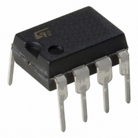
M24C02-WBN6P STMicroelectronics, M24C02-WBN6P Datasheet - Page 19

M24C02-WBN6P
Manufacturer Part Number
M24C02-WBN6P
Description
IC EEPROM 2KBIT 400KHZ 8DIP
Manufacturer
STMicroelectronics
Datasheets
1.M24C01-WMN6TP.pdf
(39 pages)
2.M24C02-WBN6P.pdf
(10 pages)
3.M24C02-WBN6P.pdf
(28 pages)
Specifications of M24C02-WBN6P
Format - Memory
EEPROMs - Serial
Memory Type
EEPROM
Memory Size
2K (256 x 8)
Speed
400kHz
Interface
I²C, 2-Wire Serial
Voltage - Supply
2.5 V ~ 5.5 V
Operating Temperature
-40°C ~ 85°C
Package / Case
8-DIP (0.300", 7.62mm)
Organization
256 K x 8
Interface Type
I2C
Maximum Clock Frequency
0.4 MHz
Access Time
900 ns
Supply Voltage (max)
5.5 V
Supply Voltage (min)
2.5 V
Maximum Operating Current
2 mA
Maximum Operating Temperature
+ 85 C
Mounting Style
Through Hole
Minimum Operating Temperature
- 40 C
Operating Supply Voltage
6.5 V
Capacitance, Input
8 pF (SDA), 6 pF (Other Pins)
Current, Input, Leakage
±2 μA
Current, Operating
2 mA
Current, Output, Leakage
±2
Data Retention
>40 yrs.
Density
2K
Package Type
PDIP8
Temperature, Operating
-40 to +85 °C
Time, Access
900 ns
Time, Fall
50 ns
Time, Rise
50 ns
Voltage, Esd
4000 V
Voltage, Input, High
3.5 to 6.5 V
Voltage, Input, Low
0.75 to 1.65 V
Voltage, Output, Low
0.4 V
Voltage, Supply
2.5 to 5.5 V
Memory Configuration
256 X 8
Clock Frequency
400kHz
Supply Voltage Range
2.5V To 5.5V
Memory Case Style
DIP
No. Of Pins
8
Rohs Compliant
Yes
Lead Free Status / RoHS Status
Lead free / RoHS Compliant
Other names
497-8584-5
M24C02-WBN6P
M24C02-WBN6P
Available stocks
Company
Part Number
Manufacturer
Quantity
Price
Part Number:
M24C02-WBN6P
Manufacturer:
ST
Quantity:
20 000
Table 13. AC Characteristics (M24Cxx-W)
Note: 1. For a reSTART condition, or following a Write cycle.
Table 14. AC Characteristics (M24Cxx-R)
Note: 1. For a reSTART condition, or following a Write cycle.
Symbol
Symbol
t
t
DL1DL2
t
t
DL1DL2
t
t
CHDX
t
CHDX
t
t
t
t
t
t
CLQV
t
t
t
t
t
t
CLQV
t
t
t
DXCX
CHDH
DXCX
CHDH
CHCL
CLCH
CLDX
CLQX
DHDL
CHCL
CLCH
CLDX
CLQX
DHDL
DLCL
t
DLCL
W
t
f
f
W
C
2. Sampled only, not 100% tested.
3. To avoid spurious START and STOP conditions, a minimum delay is placed between SCL=1 and the falling or rising edge of SDA.
4. Previous devices bearing the process letter “L” in the package marking guarantee a maximum write time of 10ms. For more infor-
C
2. Sampled only, not 100% tested.
3. To avoid spurious START and STOP conditions, a minimum delay is placed between SCL=1 and the falling or rising edge of SDA.
4. This is preliminary information.
4
3
3
1
mation about these devices and their device identification, please ask your ST Sales Office for Process Change Notices PCN MPG/
EE/0061 and 0062 (PCEE0061 and PCEE0062).
1
2
2
t
t
t
t
t
t
t
t
t
t
SU:STO
SU:STO
SU:DAT
HD:DAT
SU:STA
HD:STA
SU:DAT
HD:DAT
SU:STA
HD:STA
t
t
t
t
Alt.
f
t
Alt.
f
t
HIGH
t
HIGH
t
LOW
t
LOW
t
t
BUF
t
BUF
SCL
SCL
WR
WR
t
DH
AA
t
DH
AA
F
F
Clock Frequency
Clock Pulse Width High
Clock Pulse Width Low
SDA Fall Time
Data In Set Up Time
Data In Hold Time
Data Out Hold Time
Clock Low to Next Data Valid (Access Time)
Start Condition Set Up Time
Start Condition Hold Time
Stop Condition Set Up Time
Time between Stop Condition and Next Start Condition
Write Time
Test conditions specified in
Test conditions specified in
Parameter
Parameter
M24C16, M24C08, M24C04, M24C02, M24C01
Table 6.
Table 7.
and
and
Table 11.
Table 10.
Min.
1300
1300
1300
1300
Min.
600
100
200
200
600
600
600
600
100
200
200
600
600
600
20
20
0
0
4
Max.
Max.
400
300
900
400
300
900
10
5
4
Unit
Unit
kHz
kHz
ms
ms
ns
ns
ns
ns
ns
ns
ns
ns
ns
ns
ns
ns
ns
ns
ns
ns
ns
ns
ns
ns
ns
ns
19/28


