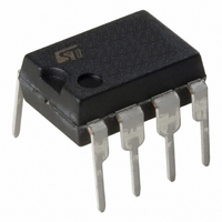
M24C02-WBN6P STMicroelectronics, M24C02-WBN6P Datasheet - Page 5

M24C02-WBN6P
Manufacturer Part Number
M24C02-WBN6P
Description
IC EEPROM 2KBIT 400KHZ 8DIP
Manufacturer
STMicroelectronics
Datasheets
1.M24C01-WMN6TP.pdf
(39 pages)
2.M24C02-WBN6P.pdf
(10 pages)
3.M24C02-WBN6P.pdf
(28 pages)
Specifications of M24C02-WBN6P
Format - Memory
EEPROMs - Serial
Memory Type
EEPROM
Memory Size
2K (256 x 8)
Speed
400kHz
Interface
I²C, 2-Wire Serial
Voltage - Supply
2.5 V ~ 5.5 V
Operating Temperature
-40°C ~ 85°C
Package / Case
8-DIP (0.300", 7.62mm)
Organization
256 K x 8
Interface Type
I2C
Maximum Clock Frequency
0.4 MHz
Access Time
900 ns
Supply Voltage (max)
5.5 V
Supply Voltage (min)
2.5 V
Maximum Operating Current
2 mA
Maximum Operating Temperature
+ 85 C
Mounting Style
Through Hole
Minimum Operating Temperature
- 40 C
Operating Supply Voltage
6.5 V
Capacitance, Input
8 pF (SDA), 6 pF (Other Pins)
Current, Input, Leakage
±2 μA
Current, Operating
2 mA
Current, Output, Leakage
±2
Data Retention
>40 yrs.
Density
2K
Package Type
PDIP8
Temperature, Operating
-40 to +85 °C
Time, Access
900 ns
Time, Fall
50 ns
Time, Rise
50 ns
Voltage, Esd
4000 V
Voltage, Input, High
3.5 to 6.5 V
Voltage, Input, Low
0.75 to 1.65 V
Voltage, Output, Low
0.4 V
Voltage, Supply
2.5 to 5.5 V
Memory Configuration
256 X 8
Clock Frequency
400kHz
Supply Voltage Range
2.5V To 5.5V
Memory Case Style
DIP
No. Of Pins
8
Rohs Compliant
Yes
Lead Free Status / RoHS Status
Lead free / RoHS Compliant
Other names
497-8584-5
M24C02-WBN6P
M24C02-WBN6P
Available stocks
Company
Part Number
Manufacturer
Quantity
Price
Part Number:
M24C02-WBN6P
Manufacturer:
ST
Quantity:
20 000
SIGNAL DESCRIPTION
Serial Clock (SCL)
This input signal is used to strobe all data in and
out of the device. In applications where this signal
is used by slave devices to synchronize the bus to
a slower clock, the bus master must have an open
drain output, and a pull-up resistor can be con-
nected from Serial Clock (SCL) to V
indicates how the value of the pull-up resistor can
be calculated). In most applications, though, this
method of synchronization is not employed, and
so the pull-up resistor is not necessary, provided
that the bus master has a push-pull (rather than
open drain) output.
Serial Data (SDA)
This bi-directional signal is used to transfer data in
or out of the device. It is an open drain output that
may be wire-OR’ed with other open drain or open
collector signals on the bus. A pull up resistor must
be connected from Serial Data (SDA) to V
ure 5.
tor can be calculated).
Chip Enable (E0, E1, E2)
These input signals are used to set the value that
is to be looked for on the three least significant bits
(b3, b2, b1) of the 7-bit Device Select Code. These
inputs must be tied to V
Device Select Code as shown in
Figure 4. Device Select Code
indicates how the value of the pull-up resis-
E i
M24Cxx
V CC
V SS
CC
or V
E i
M24Cxx
V CC
V SS
SS
Figure 4.
Ai11650
, to establish the
CC
.
(Figure 5.
CC
.
(Fig-
M24C16, M24C08, M24C04, M24C02, M24C01
Write Control (WC). This input signal is useful
for protecting the entire contents of the memory
from inadvertent write operations. Write opera-
tions are disabled to the entire memory array when
Write Control (WC) is driven High. When uncon-
nected, the signal is internally read as V
Write operations are allowed.
When Write Control (WC) is driven High, Device
Select and Address bytes are acknowledged,
Data bytes are not acknowledged.
Supply voltage (V
Operating supply voltage V
ing the memory and issuing instructions to it, a val-
id and stable V
voltage must be a DC voltage within the specified
[V
6.
ply voltage, it is recommended to decouple the
V
order of 10nF to 100nF) close to the V
package pins.
The V
the end of the transmission of the instruction and,
for a Write instruction, until the completion of the
internal write cycle (t
Internal Device Reset. In order to prevent inad-
vertent Write operations during Power-up, a Pow-
er On Reset (POR) circuit is included. At Power-up
(continuous rise of V
spond to any instruction until V
Power On Reset threshold voltage (this threshold
is lower than the minimum V
defined in
When V
vice is reset and in the Standby Power mode
Power-down. At Power-down (where V
creases continuously), as soon as V
the operating voltage range below the Power On
Reset threshold voltage, the device stops re-
sponding to any instruction sent to it.
During Power-down, the device must be deselect-
ed and in the Standby Power mode (that is there
should be no internal Write cycle in progress).
CC
CC
and
(min), V
line with a suitable capacitor (usually of the
CC
Table 7.
CC
voltage must remain stable and valid until
Table 6.
has passed the POR threshold, the de-
CC
In order to secure a stable DC sup-
(max)] range, as defined in
CC
CC
and
voltage must be applied: this
W
CC
)
).
Table
), the device does not re-
CC
CC
7.).
CC
. Prior to select-
operating voltage
has reached the
CC
drops from
CC
IL
CC
Table
, and
/V
5/28
de-
SS


