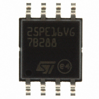
M25PE16-VMW6TG NUMONYX, M25PE16-VMW6TG Datasheet - Page 8

M25PE16-VMW6TG
Manufacturer Part Number
M25PE16-VMW6TG
Description
IC FLASH 16MBIT 75MHZ 8SOIC
Manufacturer
NUMONYX
Series
Forté™r
Datasheet
1.M45PE16-VMP6TG.pdf
(58 pages)
Specifications of M25PE16-VMW6TG
Format - Memory
FLASH
Memory Type
FLASH
Memory Size
16M (2M x 8)
Speed
75MHz
Interface
SPI, 3-Wire Serial
Voltage - Supply
2.7 V ~ 3.6 V
Operating Temperature
-40°C ~ 85°C
Package / Case
8-SOIC (5.3mm Width), 8-SOP, 8-SOEIAJ
Package
8SOIC W
Cell Type
NOR
Density
16 Mb
Architecture
Sectored
Block Organization
Symmetrical
Typical Operating Supply Voltage
3.3 V
Sector Size
64KByte x 32
Timing Type
Synchronous
Interface Type
Serial-SPI
Lead Free Status / RoHS Status
Lead free / RoHS Compliant
Other names
M25PE16-VMW6TGTR
Available stocks
Company
Part Number
Manufacturer
Quantity
Price
Company:
Part Number:
M25PE16-VMW6TG
Manufacturer:
MAXIM
Quantity:
14 500
Company:
Part Number:
M25PE16-VMW6TG
Manufacturer:
Numonyx
Quantity:
15 000
Part Number:
M25PE16-VMW6TG
Manufacturer:
ST
Quantity:
20 000
Signal descriptions
2
2.1
2.2
2.3
2.4
2.5
2.6
8/58
Signal descriptions
Serial data output (Q)
This output signal is used to transfer data serially out of the device. Data is shifted out on the
falling edge of Serial Clock (C).
Serial data input (D)
This input signal is used to transfer data serially into the device. It receives instructions,
addresses, and the data to be programmed. Values are latched on the rising edge of Serial
Clock (C).
Serial clock (C)
This input signal provides the timing of the serial interface. Instructions, addresses, or data
present at Serial Data Input (D) are latched on the rising edge of Serial Clock (C). Data on
Serial Data Output (Q) changes after the falling edge of Serial Clock (C).
Chip select (S)
When this input signal is High, the device is deselected and serial data output (Q) is at high
impedance. Unless an internal read, program, erase or write cycle is in progress, the device
will be in the standby mode (this is not the deep power-down mode). Driving Chip Select (S)
Low selects the device, placing it in the active power mode.
After power-up, a falling edge on Chip Select (S) is required prior to the start of any
instruction.
Reset (Reset)
The Reset (Reset) input provides a hardware reset for the memory.
When Reset (Reset) is driven High, the memory is in the normal operating mode. When
Reset (Reset) is driven Low, the memory will enter the reset mode. In this mode, the output
is high impedance.
Driving Reset (Reset) Low while an internal operation is in progress will affect this operation
(write, program or erase cycle) and data may be lost.
See
Write protect (W)
The write protect (W) input is used to freeze the size of the area of memory that is protected
against write, program and erase instructions (as specified by the values in the BP2, BP1
and BP0 bits of the status register). See
Table 12
for the status of the device after a Reset Low pulse.
Section 6.4: Read status register
(RDSR).
M25PE16


