CY7C1041DV33-10ZSXIT Cypress Semiconductor Corp, CY7C1041DV33-10ZSXIT Datasheet - Page 3
CY7C1041DV33-10ZSXIT
Manufacturer Part Number
CY7C1041DV33-10ZSXIT
Description
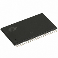
IC SRAM 4MBIT 10NS 44TSOP
Manufacturer
Cypress Semiconductor Corp
Type
Asynchronousr
Specifications of CY7C1041DV33-10ZSXIT
Memory Size
4M (256K x 16)
Package / Case
44-TSOP II
Format - Memory
RAM
Memory Type
SRAM - Asynchronous
Speed
10ns
Interface
Parallel
Voltage - Supply
3 V ~ 3.6 V
Operating Temperature
-40°C ~ 85°C
Access Time
10 ns
Supply Voltage (max)
3.6 V
Supply Voltage (min)
3 V
Maximum Operating Current
90 mA
Maximum Operating Temperature
+ 85 C
Minimum Operating Temperature
- 40 C
Mounting Style
SMD/SMT
Number Of Ports
1
Operating Supply Voltage
3.3 V
Memory Configuration
256K X 16
Supply Voltage Range
3V To 3.6V
Memory Case Style
TSOP
No. Of Pins
44
Operating Temperature Range
-40°C To +85°C
Density
4Mb
Access Time (max)
10ns
Sync/async
Asynchronous
Architecture
SDR
Clock Freq (max)
Not Required
Operating Supply Voltage (typ)
3.3V
Address Bus
18b
Operating Temp Range
-40C to 85C
Supply Current
90mA
Operating Supply Voltage (min)
3V
Operating Supply Voltage (max)
3.6V
Operating Temperature Classification
Industrial
Mounting
Surface Mount
Pin Count
44
Word Size
16b
Number Of Words
256Kword
Lead Free Status / RoHS Status
Lead free / RoHS Compliant
Lead Free Status / RoHS Status
Lead free / RoHS Compliant, Lead free / RoHS Compliant
Available stocks
Company
Part Number
Manufacturer
Quantity
Price

Part Number:
CY7C1041DV33-10ZSXIT
Manufacturer:
CYPRESS/赛普拉斯
Quantity:
20 000


Selection Guide
Pin Configuration
Notes
Document Number: 38-05473 Rev. *I
Maximum access time
Maximum operating current
Maximum CMOS standby current
2. Automotive product information is preliminary.
3. NC pins are not connected on the die.
4. Pinout 1 is compliant with CY7C1041CV33 and pinout 2 is JEDEC compliant. The difference between the two is that the higher and lower byte I/Os (I/O
balls) are swapped.
Description
Figure 1. 48-ball VFBGA (Pinout 1)
BLE
IO
IO
V
V
IO
IO
NC
SS
CC
1
6
7
0
1
BHE
IO
IO
OE
IO
NC
IO
A
2
2
8
4
5
3
A
A
NC
A
A
A
A
A
3
17
14
12
0
3
5
9
A
A
A
A
A
A
A
A
4
15
13
10
1
4
7
16
6
IO
IO
IO
CE
IO
WE
A
–10 (Industrial)
A
5
11
12
2
13
10
11
V
IO
IO
IO
V
IO
NC
NC
CC
6
SS
10
90
10
14
15
8
9
[3, 4]
Figure 3. 44-pin SOJ/TSOP II
B
C
D
E
F
G
H
A
V
V
WE
IO
IO
IO
IO
IO
IO
IO
IO
A
A
A
A
A
CE
A
A
A
A
A
CC
SS
5
6
7
8
9
0
1
2
3
4
0
1
2
3
4
5
6
7
10
11
12
13
14
15
16
17
18
19
20
21
22
1
2
3
4
5
6
7
8
9
–10 (Automotive-A)
44
43
42
41
40
39
38
37
36
35
34
33
32
31
30
29
28
27
26
25
24
23
10
90
10
A
BHE
BLE
IO
IO
V
V
IO
IO
IO
A
A
A
A
A
A
OE
IO
IO
IO
NC
A
16
SS
14
11
10
17
15
CC
13
12
14
13
12
11
10
9
8
15
Figure 2. 48-ball VFBGA (Pinout 2)
BLE
IO
IO
V
V
IO
IO
NC
CC
SS
1
14
15
8
9
[2]
BHE
IO
IO
IO
OE
NC
IO
A
2
10
8
12
–12 (Automotive-E)
11
13
A
A
NC
A
A
A
A
A
3
17
14
12
0
3
5
9
A
A
A
12
95
15
A
A
A
A
A
4
15
13
10
7
16
1
4
6
IO
IO
CE
IO
WE
A
IO
A
CY7C1041DV33
5
11
2
5
3
4
1
[2]
V
IO
IO
IO
NC
IO
V
NC
CC
6
SS
6
0
7
2
[3, 4]
Page 3 of 17
B
C
D
E
F
G
H
[7:0]
A
Unit
mA
mA
ns
and I/O
[15:8]
[+] Feedback
Related parts for CY7C1041DV33-10ZSXIT
Image
Part Number
Description
Manufacturer
Datasheet
Request
R

Part Number:
Description:
CY7C1041DV33-10BVJXI
Manufacturer:
Cypress Semiconductor Corp
Datasheet:
Part Number:
Description:
CY7C1041DV33-10BVJXIT
Manufacturer:
Cypress Semiconductor Corp
Datasheet:
Part Number:
Description:
CY7C1041DV33-10BVXIT
Manufacturer:
Cypress Semiconductor Corp
Datasheet:

Part Number:
Description:
CY7C1041DV33-10VXIT
Manufacturer:
Cypress Semiconductor Corp
Datasheet:

Part Number:
Description:
IC SRAM 4MBIT 10NS 44TSOP
Manufacturer:
Cypress Semiconductor Corp
Datasheet:
Part Number:
Description:
IC SRAM 4MBIT 10NS 48VFBGA
Manufacturer:
Cypress Semiconductor Corp
Datasheet:
Part Number:
Description:
IC SRAM 4MBIT 10NS 44SOJ
Manufacturer:
Cypress Semiconductor Corp
Datasheet:
Part Number:
Description:
CY7C1041DV33-10BVI
Manufacturer:
Cypress Semiconductor Corp
Datasheet:
Part Number:
Description:
CY7C1041DV33-10BVIT
Manufacturer:
Cypress Semiconductor Corp
Datasheet:
Part Number:
Description:
IC SRAM 4MBIT 10NS 44TSOP
Manufacturer:
Cypress Semiconductor Corp
Datasheet:
Part Number:
Description:
IC SRAM 4MBIT 10NS 44SOJ
Manufacturer:
Cypress Semiconductor Corp
Datasheet:
Part Number:
Description:
CY7C1041D-10VXIT
Manufacturer:
Cypress Semiconductor Corp
Datasheet:
Part Number:
Description:
CY7C1041D-10ZSXIT
Manufacturer:
Cypress Semiconductor Corp
Datasheet:


Part Number:
Description:
4-Mbit (256K x 16) Static RAM
Manufacturer:
CYPRESS [Cypress Semiconductor]
Datasheet: