AT49LH00B4-33JC Atmel, AT49LH00B4-33JC Datasheet - Page 14
AT49LH00B4-33JC
Manufacturer Part Number
AT49LH00B4-33JC
Description
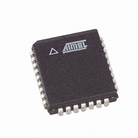
IC FLASH 4MBIT 33MHZ 32PLCC
Manufacturer
Atmel
Datasheet
1.AT49LH00B4-33JC.pdf
(41 pages)
Specifications of AT49LH00B4-33JC
Format - Memory
FLASH
Memory Type
FLASH
Memory Size
4M (512K x 8)
Speed
33MHz
Interface
Parallel
Voltage - Supply
3 V ~ 3.6 V
Operating Temperature
0°C ~ 85°C
Package / Case
32-PLCC
Lead Free Status / RoHS Status
Contains lead / RoHS non-compliant
Available stocks
Company
Part Number
Manufacturer
Quantity
Price
Company:

Part Number:
AT49LH00B4-33JC
Manufacturer:
ATMEL
Quantity:
975


7.6.4
7.6.5
7.6.6
14
AT49LH00B4
Additional Fields for LPC Memory Cycles
TAR (Turn-around) Field
SYNC (Synchronize) Field
strapped values are internally inverted. For example, if ID3 was strapped to GND, a logical value
of 1 would be compared against address bit A22. If the inverted states of the ID[3:0] pins match
with address bits A22 - A19, then the device will continue to decode the rest of cycle (see LPC
Multiple Device Selection for mode details).
Addresses are transferred to the device with the most significant nibble first.
Additional fields are required to complete an LPC read or write cycle. The placement of these
fields, in addition to the data field, depends on whether the cycle is an LPC read or write. The
LPC Read Cycle and LPC Write Cycle sections detail the order of the various fields.
This 2-clock field is driven by the master when it is turning control over to the LPC memory
device, and it is driven by the LPC device when it is turning control back over to the master. On
the first clock of the TAR field, the master or LPC device drives the FWH/LAD[3:0] lines to
1111b. On the second clock, the master or LPC device puts the FWH/LAD[3:0] lines into a high-
impedance state.
This field is used to add wait-states for an access. It can be several clocks in length. On target
cycles, this field is driven by the LPC memory device. If the LPC device needs to assert wait-
states, it does so by driving a “wait” SYNC value of 0101b on the FWH/LAD[3:0] pins until it is
ready. When ready, the device will drive a “ready” SYNC value of 0000b on the FWH/LAD[3:0]
lines. Valid values for the SYNC field are shown in
Table 7-6.
SYNC Value
0000b
0101b
Valid SYNC Values
SYNC Type
RSYNC (Ready SYNC) – Synchronization has been achieved with no error.
WSYNC (Wait SYNC) – Device is indicating wait-states (also referred to as
short-sync).
Table
7-6.
3379C–FLASH–3/05
Related parts for AT49LH00B4-33JC
Image
Part Number
Description
Manufacturer
Datasheet
Request
R

Part Number:
Description:
DEV KIT FOR AVR/AVR32
Manufacturer:
Atmel
Datasheet:

Part Number:
Description:
INTERVAL AND WIPE/WASH WIPER CONTROL IC WITH DELAY
Manufacturer:
ATMEL Corporation
Datasheet:
Part Number:
Description:
Low-Voltage Voice-Switched IC for Hands-Free Operation
Manufacturer:
ATMEL Corporation
Datasheet:
Part Number:
Description:
MONOLITHIC INTEGRATED FEATUREPHONE CIRCUIT
Manufacturer:
ATMEL Corporation
Datasheet:
Part Number:
Description:
AM-FM Receiver IC U4255BM-M
Manufacturer:
ATMEL Corporation
Datasheet:
Part Number:
Description:
Monolithic Integrated Feature Phone Circuit
Manufacturer:
ATMEL Corporation
Datasheet:
Part Number:
Description:
Multistandard Video-IF and Quasi Parallel Sound Processing
Manufacturer:
ATMEL Corporation
Datasheet:
Part Number:
Description:
High-performance EE PLD
Manufacturer:
ATMEL Corporation
Datasheet:
Part Number:
Description:
8-bit Flash Microcontroller
Manufacturer:
ATMEL Corporation
Datasheet:
Part Number:
Description:
2-Wire Serial EEPROM
Manufacturer:
ATMEL Corporation
Datasheet: