AT49LH00B4-33JC Atmel, AT49LH00B4-33JC Datasheet - Page 23
AT49LH00B4-33JC
Manufacturer Part Number
AT49LH00B4-33JC
Description
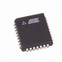
IC FLASH 4MBIT 33MHZ 32PLCC
Manufacturer
Atmel
Datasheet
1.AT49LH00B4-33JC.pdf
(41 pages)
Specifications of AT49LH00B4-33JC
Format - Memory
FLASH
Memory Type
FLASH
Memory Size
4M (512K x 8)
Speed
33MHz
Interface
Parallel
Voltage - Supply
3 V ~ 3.6 V
Operating Temperature
0°C ~ 85°C
Package / Case
32-PLCC
Lead Free Status / RoHS Status
Contains lead / RoHS non-compliant
Available stocks
Company
Part Number
Manufacturer
Quantity
Price
Company:

Part Number:
AT49LH00B4-33JC
Manufacturer:
ATMEL
Quantity:
975


12. General-Purpose Input Register
13. Multiple Device Selection
13.1
3379C–FLASH–3/05
FWH Multiple Device Selection
A General-purpose Input Register is provided to read the status of the GPI[4:0] pins when using
the FWH/LPC interface. Since this is a pass-through register, there is no default value. It is rec-
ommended that the GPI[4:0] pins be in their desired state before FWH4/LFRAME is brought low
for the beginning of the next bus cycle and remain in that state until the end of the cycle.
Table 12-1.
Table 12-2.
Multiple devices may be used in a system to increase the overall memory density. By using the
four ID strapping pins, ID[3:0], up to 16 devices may be attached to the same bus. BIOS support,
bus loading, or the attaching bridge may limit the actual number of devices that can be con-
nected to the bus.
The boot device must have ID[3:0] equal to 0000b, and all subsequent devices should use
sequential up-count strapping.
The strapping values on ID[3:0] must match the values in the IDSEL field when performing FWH
memory cycles. The device will compare the values on the ID[3:0] pins with the IDSEL field. If
there is a mismatch, the device will ignore the remainder of the cycle. The device will then enter
standby mode when the FWH4/LFRAME pin is high and no internal operation is in progress. The
FWH/LAD[3:0] pins will also be placed in a high-impedance state.
Register Name
Bit
7:5
GPI_REG
4
3
2
1
0
GPI Register Memory Address
General-purpose Input Register
GPI_REG4
GPI_REG3
GPI_REG2
GPI_REG1
GPI_REG0
Reserved
Associated Pins
Name
GPI[4:0]
Description
Reserved for future use.
0
1
0
1
0
1
0
1
0
1
FFBC0100H
FWH Mode
Register Memory Address
GPI4 input pin is at V
GPI4 input pin is at V
GPI3 input pin is at V
GPI3 input pin is at V
GPI2 input pin is at V
GPI2 input pin is at V
GPI1 input pin is at V
GPI1 input pin is at V
GPI0 input pin is at V
GPI0 input pin is at V
FF7C0100H
LPC Mode
IL
IH
IL
IH
IL
IH
IL
IH
IL
IH
.
.
.
.
.
.
.
.
.
.
AT49LH00B4
Register Type
Read Only
23
Related parts for AT49LH00B4-33JC
Image
Part Number
Description
Manufacturer
Datasheet
Request
R

Part Number:
Description:
DEV KIT FOR AVR/AVR32
Manufacturer:
Atmel
Datasheet:

Part Number:
Description:
INTERVAL AND WIPE/WASH WIPER CONTROL IC WITH DELAY
Manufacturer:
ATMEL Corporation
Datasheet:
Part Number:
Description:
Low-Voltage Voice-Switched IC for Hands-Free Operation
Manufacturer:
ATMEL Corporation
Datasheet:
Part Number:
Description:
MONOLITHIC INTEGRATED FEATUREPHONE CIRCUIT
Manufacturer:
ATMEL Corporation
Datasheet:
Part Number:
Description:
AM-FM Receiver IC U4255BM-M
Manufacturer:
ATMEL Corporation
Datasheet:
Part Number:
Description:
Monolithic Integrated Feature Phone Circuit
Manufacturer:
ATMEL Corporation
Datasheet:
Part Number:
Description:
Multistandard Video-IF and Quasi Parallel Sound Processing
Manufacturer:
ATMEL Corporation
Datasheet:
Part Number:
Description:
High-performance EE PLD
Manufacturer:
ATMEL Corporation
Datasheet:
Part Number:
Description:
8-bit Flash Microcontroller
Manufacturer:
ATMEL Corporation
Datasheet:
Part Number:
Description:
2-Wire Serial EEPROM
Manufacturer:
ATMEL Corporation
Datasheet: