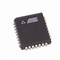
AT49LH00B4-33JC Atmel, AT49LH00B4-33JC Datasheet - Page 25

AT49LH00B4-33JC
Manufacturer Part Number
AT49LH00B4-33JC
Description
IC FLASH 4MBIT 33MHZ 32PLCC
Manufacturer
Atmel
Datasheet
1.AT49LH00B4-33JC.pdf
(41 pages)
Specifications of AT49LH00B4-33JC
Format - Memory
FLASH
Memory Type
FLASH
Memory Size
4M (512K x 8)
Speed
33MHz
Interface
Parallel
Voltage - Supply
3 V ~ 3.6 V
Operating Temperature
0°C ~ 85°C
Package / Case
32-PLCC
Lead Free Status / RoHS Status
Contains lead / RoHS non-compliant
Available stocks
Company
Part Number
Manufacturer
Quantity
Price
Company:
Part Number:
AT49LH00B4-33JC
Manufacturer:
ATMEL
Quantity:
975
14. A/A Mux Interface
3379C–FLASH–3/05
Table 13-2.
The A/A Mux interface is designed as a programming interface for OEMs to use during mother-
board manufacturing or component pre-programming. The term A/A Mux refers to the
multiplexed row and column addresses that this interface utilizes. The A/A Mux interface dramat-
ically reduces the amount of overhead needed to access the device, allowing the device to be
tested and programmed quickly with automated test equipment (ATE) and PROM programmers
in the OEM’s manufacturing flow. The number of signals required to use the interface does not
change with device density; therefore, the interface can accommodate larger density devices
while still allowing the device to fit into low lead-count packages.
Only basic read, erase, and program operations can be performed through the A/A Mux inter-
face; FWH/LPC features, such as the use of the Sector Locking Registers and the General-
purpose Input Register, are not available.
The A/A Mux interface mode is selected by driving the IC control pin high. The IC pin is internally
pulled down in the device, so a modest amount of leakage current should be expected to be
drawn (see DC Specifications) when the pin is driven high.
Four control pins dictate the flow of data into and out of the device: R/C, OE, WE, and RST. The
R/C pin is the A/A Mux interface control pin used to latch row and column addresses. OE is the
data output control pin for the I/O[7:0] lines and, when active, drives the selected memory data
onto the I/O bus (WE and RST must be at VIH). The WE pin controls the flow of data into the
device. Addresses previously captured by the R/C pin transitions and data are latched into the
device on the rising edge of WE. The RST pin is used to reset the device.
0 (Boot Device)
Device
10
11
12
13
14
15
1
2
3
4
5
6
7
8
9
LPC Multiple Device Selection
ID3
0
0
0
0
0
0
0
0
1
1
1
1
1
1
1
1
ID2
ID Strapping Pins
0
0
0
0
1
1
1
1
0
0
0
0
1
1
1
1
ID1
0
0
1
1
0
0
1
1
0
0
1
1
0
0
1
1
ID0
0
1
0
1
0
1
0
1
0
1
0
1
0
1
0
1
AT49LH00B4
Address Bits
A22-A19
1111b
1110b
1101b
1100b
1011b
1010b
1001b
1000b
0111b
0110b
0101b
0100b
0011b
0010b
0001b
0000b
25


