AT49LH00B4-33JC Atmel, AT49LH00B4-33JC Datasheet - Page 26
AT49LH00B4-33JC
Manufacturer Part Number
AT49LH00B4-33JC
Description
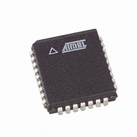
IC FLASH 4MBIT 33MHZ 32PLCC
Manufacturer
Atmel
Datasheet
1.AT49LH00B4-33JC.pdf
(41 pages)
Specifications of AT49LH00B4-33JC
Format - Memory
FLASH
Memory Type
FLASH
Memory Size
4M (512K x 8)
Speed
33MHz
Interface
Parallel
Voltage - Supply
3 V ~ 3.6 V
Operating Temperature
0°C ~ 85°C
Package / Case
32-PLCC
Lead Free Status / RoHS Status
Contains lead / RoHS non-compliant
Available stocks
Company
Part Number
Manufacturer
Quantity
Price
Company:

Part Number:
AT49LH00B4-33JC
Manufacturer:
ATMEL
Quantity:
975


14.1
14.2
14.3
14.4
15. Device Operation
26
Bus Operation
Output Disable/Enable
ROW/Column Addresses
RDY/BSY:
AT49LH00B4
All A/A Mux bus cycles can be conformed to operate on most automated test equipment and
PROM programmers.
Table 14-1.
Notes:
With OE at a logic-high level (V
placed in the high-impedance state. With OE at a logic-low level (V
enabled. Output pins I/O[7:0] are placed in an output-drive state.
R/C is the A/A Mux interface control pin used to latch row (A10 - A0) and column address (A18 -
A11) values presented on the A[10:0] pins. R/C latches row addresses on the falling edge and
column addresses on the rising edge.
The open-drain Ready/Busy output pin provides a hardware method of detecting the end of a
program or erase operation. RDY/BSY is actively pulled low during the internal program and
erase cycles and is released at the completion of the cycle.
The FWH/LPC and A/A Mux interfaces should be considered hardware interfaces that can be
used to transfer commands and data to and from the device. The device commands detailed in
Table 16.
Since the FWH/LPC interface communicates using a 4-bit data bus and the A/A Mux interface
utilizes an 8-bit data bus, the number of interface bus cycles needed to perform an operation will
vary. For example, when using the FWH/LPC interface, 17 PCI clock cycles are required for a
FWH or LPC memory write cycle. Therefore, for one “write” device command cycle,
17 FWH/LPC bus cycles are needed. Likewise, for one “read” device command cycle using the
FWH/LPC interface, 19 FWH/LPC bus cycles are required.
Mode
Read
Output Disable
Write
Product ID Read
(1)(2)
(1)(2)
1. X can be V
2. V
3. Refer to
can be issued using either interface.
V
IH
IL
min = 0.5V, V
(1)(2)
and V
A/A Mux Interface Bus Operations
(1)(2)(3)
Table 16-2
IL
IL
refer to the DC characteristics associated with the Flash memory output buffers:
or V
IL
IH
max = 0.8V, V
for control and address input pins.
for Product ID addresses and data.
RST
V
V
V
V
IH
IH
IH
IH
IH
), the device outputs are disabled. Output pins I/O[7:0] are
IH
min = 2.0V, V
OE
V
V
V
V
IH
IH
IL
IL
IH
max = V
WE
V
V
V
V
IH
IH
IH
IL
CC
+ 0.5V.
Address
IL
Note 3
), the device outputs are
X
X
X
3379C–FLASH–3/05
I/O[7:0]
High-Z
Note 3
D
D
OUT
IN
Related parts for AT49LH00B4-33JC
Image
Part Number
Description
Manufacturer
Datasheet
Request
R

Part Number:
Description:
DEV KIT FOR AVR/AVR32
Manufacturer:
Atmel
Datasheet:

Part Number:
Description:
INTERVAL AND WIPE/WASH WIPER CONTROL IC WITH DELAY
Manufacturer:
ATMEL Corporation
Datasheet:
Part Number:
Description:
Low-Voltage Voice-Switched IC for Hands-Free Operation
Manufacturer:
ATMEL Corporation
Datasheet:
Part Number:
Description:
MONOLITHIC INTEGRATED FEATUREPHONE CIRCUIT
Manufacturer:
ATMEL Corporation
Datasheet:
Part Number:
Description:
AM-FM Receiver IC U4255BM-M
Manufacturer:
ATMEL Corporation
Datasheet:
Part Number:
Description:
Monolithic Integrated Feature Phone Circuit
Manufacturer:
ATMEL Corporation
Datasheet:
Part Number:
Description:
Multistandard Video-IF and Quasi Parallel Sound Processing
Manufacturer:
ATMEL Corporation
Datasheet:
Part Number:
Description:
High-performance EE PLD
Manufacturer:
ATMEL Corporation
Datasheet:
Part Number:
Description:
8-bit Flash Microcontroller
Manufacturer:
ATMEL Corporation
Datasheet:
Part Number:
Description:
2-Wire Serial EEPROM
Manufacturer:
ATMEL Corporation
Datasheet: