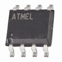
AT45DB081D-SU Atmel, AT45DB081D-SU Datasheet - Page 24

AT45DB081D-SU
Manufacturer Part Number
AT45DB081D-SU
Description
IC FLASH 8MBIT 66MHZ 8SOIC
Manufacturer
Atmel
Specifications of AT45DB081D-SU
Format - Memory
FLASH
Memory Type
DataFLASH
Memory Size
8M (4096 pages x 264 bytes)
Speed
66MHz
Interface
SPI, RapidS
Voltage - Supply
2.7 V ~ 3.6 V
Operating Temperature
-40°C ~ 85°C
Package / Case
8-SOIC (5.3mm Width), 8-SOP, 8-SOEIAJ
Architecture
Sectored
Interface Type
SPI
Supply Voltage (max)
3.6 V
Supply Voltage (min)
2.7 V
Maximum Operating Current
15 mA
Mounting Style
SMD/SMT
Organization
64 KB x 16
Memory Configuration
4096 Pages X 264 Bytes
Clock Frequency
50MHz
Supply Voltage Range
2.5V To 3.6V, 2.7V To 3.6V
Rohs Compliant
Yes
Lead Free Status / RoHS Status
Lead free / RoHS Compliant
Available stocks
Company
Part Number
Manufacturer
Quantity
Price
Company:
Part Number:
AT45DB081D-SU
Manufacturer:
ATMEL
Quantity:
750
Company:
Part Number:
AT45DB081D-SU
Manufacturer:
ATMEL
Quantity:
8
Part Number:
AT45DB081D-SU
Manufacturer:
ATMEL/爱特梅尔
Quantity:
20 000
Part Number:
AT45DB081D-SU-2.5
Manufacturer:
ATMEL/爱特梅尔
Quantity:
20 000
13.1
14. Manufacturer and Device ID Read
24
Programming the Configuration Register
Atmel AT45DB081D
To program the Configuration Register for “power of 2” binary page size, the CS pin must first be
asserted as it would be with any other command. Once the CS pin has been asserted, the
appropriate 4-byte opcode sequence must be clocked into the device in the correct order. The
4-byte opcode sequence must start with 3DH and be followed by 2AH, 80H, and A6H. After the
last bit of the opcode sequence has been clocked in, the CS pin must be deasserted to initiate
the internally self-timed program cycle. The programming of the Configuration Register should
take place in a time of t
busy. The device must be power-cycled after the completion of the program cycle to set the
“power of 2” page size. If the device is powered-down before the completion of the program
cycle, then setting the Configuration Register cannot be guaranteed. However, the user should
check bit zero of the status register to see whether the page size was configured for binary page
size. If not, the command can be re-issued again.
Table 13-1.
Figure 13-1. Program Configuration Register
Identification information can be read from the device to enable systems to electronically query
and identify the device while it is in system. The identification method and the command opcode
comply with the JEDEC standard for “Manufacturer and Device ID Read Methodology for SPI
Compatible Serial Interface Memory Devices”. The type of information that can be read from the
device includes the JEDEC defined Manufacturer ID, the vendor specific Device ID, and the ven-
dor specific Extended Device Information.
To read the identification information, the CS pin must first be asserted and the opcode of 9FH
must be clocked into the device. After the opcode has been clocked in, the device will begin out-
putting the identification data on the SO pin during the subsequent clock cycles. The first byte
that will be output will be the Manufacturer ID followed by two bytes of Device ID information.
The fourth byte output will be the Extended Device Information String Length, which will be 00H
indicating that no Extended Device Information follows. As indicated in the JEDEC standard,
reading the Extended Device Information String Length and any subsequent data is optional.
Deasserting the CS pin will terminate the Manufacturer and Device ID Read operation and put
the SO pin into a high-impedance state. The CS pin can be deasserted at any time and does not
require that a full byte of data be read.
Command
Power of Two Page Size
Programming the Configuration Register
CS
SI
P
Each transition
represents 8 bits
, during which time the Status Register will indicate that the device is
Opcode
Byte 1
Opcode
Byte 2
Byte 1
3DH
Opcode
Byte 3
Opcode
Byte 2
Byte 4
2AH
Byte 3
80H
3596M–DFLASH–5/10
Byte 4
A6H


