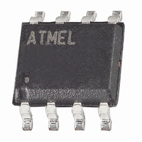
AT45DB041D-SSU Atmel, AT45DB041D-SSU Datasheet - Page 15

AT45DB041D-SSU
Manufacturer Part Number
AT45DB041D-SSU
Description
IC FLASH 4MBIT 66MHZ 8SOIC
Manufacturer
Atmel
Specifications of AT45DB041D-SSU
Format - Memory
FLASH
Memory Type
DataFLASH
Memory Size
4M (2048 pages x 264 bytes)
Speed
66MHz
Interface
SPI, RapidS
Voltage - Supply
2.7 V ~ 3.6 V
Operating Temperature
-40°C ~ 85°C
Package / Case
8-SOIC (3.9mm Width)
Density
4Mb
Access Time (max)
6ns
Interface Type
Serial (SPI)
Boot Type
Not Required
Address Bus
1b
Operating Supply Voltage (typ)
3/3.3V
Operating Temp Range
-40C to 85C
Package Type
SOIC
Program/erase Volt (typ)
2.7 to 3.6V
Sync/async
Synchronous
Operating Temperature Classification
Industrial
Operating Supply Voltage (min)
2.7V
Operating Supply Voltage (max)
3.6V
Supply Current
15mA
Mounting
Surface Mount
Pin Count
8
Architecture
Sectored
Supply Voltage (max)
3.6 V
Supply Voltage (min)
2.7 V
Maximum Operating Current
15 mA
Mounting Style
SMD/SMT
Organization
64 KB x 8
Memory Configuration
2048 Pages X 256 Bytes
Clock Frequency
50MHz
Supply Voltage Range
2.7V To 3.6V
Memory Case Style
SOIC
Rohs Compliant
Yes
Lead Free Status / RoHS Status
Lead free / RoHS Compliant
Available stocks
Company
Part Number
Manufacturer
Quantity
Price
Company:
Part Number:
AT45DB041D-SSU
Manufacturer:
ATMEL
Quantity:
12 000
Part Number:
AT45DB041D-SSU
Manufacturer:
ATMEL/爱特梅尔
Quantity:
20 000
Part Number:
AT45DB041D-SSU-2.5
Manufacturer:
ATMEL/爱特梅尔
Quantity:
20 000
9.1.1
3595P–DFLASH–09/09
Erase Sector Protection Register Command
In order to modify and change the values of the Sector Protection Register, it must first be
erased using the Erase Sector Protection Register command.
To erase the Sector Protection Register, the CS pin must first be asserted as it would be with
any other command. Once the CS pin has been asserted, the appropriate 4-byte opcode
sequence must be clocked into the device via the SI pin. The 4-byte opcode sequence must
start with 3DH and be followed by 2AH, 7FH, and CFH. After the last bit of the opcode sequence
has been clocked in, the CS pin must be deasserted to initiate the internally self-timed erase
cycle. The erasing of the Sector Protection Register should take place in a time of t
which time the Status Register will indicate that the device is busy. If the device is powered-
down before the completion of the erase cycle, then the contents of the Sector Protection Regis-
ter cannot be guaranteed.
The Sector Protection Register can be erased with the sector protection enabled or disabled.
Since the erased state (FFH) of each byte in the Sector Protection Register is used to indicate
that a sector is specified for protection, leaving the sector protection enabled during the erasing
of the register allows the protection scheme to be more effective in the prevention of accidental
programming or erasing of the device. If for some reason an erroneous program or erase com-
mand is sent to the device immediately after erasing the Sector Protection Register and before
the register can be reprogrammed, then the erroneous program or erase command will not be
processed because all sectors would be protected.
Figure 9-2.
Command
Erase Sector Protection Register
Erase Sector Protection Register
CS
SI
Each transition
represents 8 bits
Opcode
Byte 1
Byte 1
Opcode
Byte 2
3DH
Opcode
Byte 3
Byte 2
2AH
Opcode
Byte 4
AT45DB041D
Byte 3
7FH
Byte 4
PE
CFH
, during
15


